PCB slice and preparation method thereof

A technology of slicing and prepreg, which is used in multilayer circuit manufacturing, printed circuit manufacturing, printed circuit components and other directions, which can solve the problem of copper tearing in hole wall pits, slow down the drilling feed speed and retract speed, and increase frictional heat. and other problems, to achieve the effect of improving production efficiency, prolonging the life of the drill bit, and prolonging the life of the drill.

Active Publication Date: 2014-11-19
大连崇达电子有限公司
View PDF4 Cites 6 Cited by
  • Summary
  • Abstract
  • Description
  • Claims
  • Application Information

AI Technical Summary

Problems solved by technology

The existing manufacturing method of slicing holes has the following defects: because there are many copper layers and the total copper thickness is relatively thick, the frictional heat generated between the metal drill needle and copper during drilling is more, which will lead to pits on the hole wall and copper tearing, etc. Problem: When the aperture of the slicing hole is small (generally less than 0.45mm), the metal drill is easily broken due to more copper layers and a thicker total copper thickness; in addition, in order to reduce the occurrence of metal drills being broken , it is necessary to slow down the feeding speed and retracting speed during drilling, which greatly affects the drilling efficiency, and when the parameters of the slice hole and the normal hole in the plate are inconsistent, the equipment program needs to be adjusted, which further affects the drilling efficiency. Pore ​​efficiency

Method used


Image

  • PCB slice and preparation method thereof
  • PCB slice and preparation method thereof
  • PCB slice and preparation method thereof

Examples


Embodiment 1

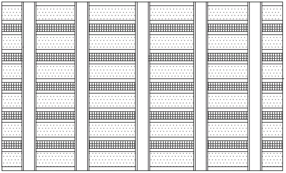
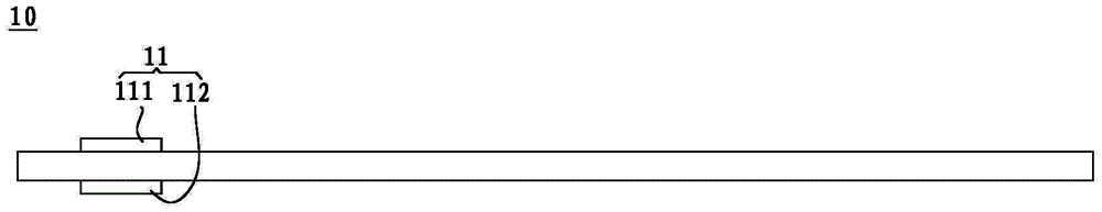
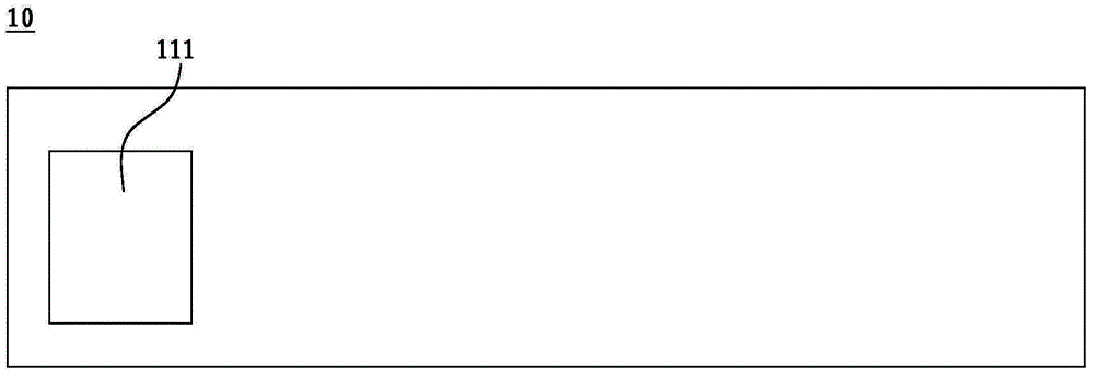
[0021] refer to Figure 2-5 , a PCB slice provided in this embodiment, including five inner layer sliced ​​boards 10, two outer layer copper foils 30, and a prepreg 40 as an adhesive material. Each inner layer slicing board 10 is provided with a copper foil drilling position 11, and the copper foil drilling position 11 includes an upper copper foil 111 and a lower copper foil 112 attached to the upper and lower surfaces of the inner layer slicing board 10; The copper foil drilling positions 11 on one inner slice board 10 are staggered from the copper foil drilling positions 11 on the other inner slice boards 10 . The outer layer copper foil 30, the inner layer slice plate 10 and the prepreg 40 are sequentially pressed together, so that the two outer layer copper foils 30 are located at the outermost layer, and the five inner layer slice plates 10 are located between the two outer layer copper foils 30, and A prepreg 40 is arranged between the outer layer copper foil 30 and th...

Embodiment 2

[0028] A PCB slicing provided in this embodiment includes 6 inner-layer slicing boards, two outer-layer copper foils and a prepreg. Each inner layer slice board is provided with a copper foil drilling position, the copper foil drill hole position includes the upper copper foil and the lower copper foil on the lower surface of the inner layer slice board; each inner layer slice board The copper foil drilling positions on the board are staggered from the copper foil drilling positions on other inner slice boards. The outer layer copper foil, the inner layer slice board and the prepreg are pressed together sequentially, so that the two outer layer copper foils are located on the outermost layer, the six inner layer slice boards are located between the two outer layer copper foils, and the outer layer copper foil and the inner layer Prepregs are arranged between the layer slicing plates and between the two inner layer slicing plates, and a slicing hole with a cross-sectional area ...


PUM


Abstract

The invention relates to the technical field of printed circuit block (PCB) manufacturing, in particular to a PCB slice and a preparation method thereof. The PCB slice is prepared by the following steps: firstly manufacturing mutually staggered copper foil drilling positions on inner-layer slice plates, and then performing pressing, slice hole drilling, copper deposition, full board plating and slicing. According to the method, in the initial design, the copper foil drilling positions are designed on the inner-layer slice plates, and the copper foil drilling positions between every two inner-layer slice plates are mutually staggered, so that each formed slice hole can penetrate the copper foil drilling position on one inner layer slice plate, the thickness of copper required to be penetrated during drilling is reduced, drilling speed does not need to be regulated to slow along with the increase of layers of PCBs, and the service life of a drill bit can be prolonged by three times; the production efficiency is improved, the cost is reduced; when the PCB slice with different PCB layers is manufactured, phenomena that concave pits on hole walls and tearing of hole copper are prevented even the knife speed is not regulated.

Description

technical field [0001] The invention relates to the technical field of printed circuit board production, in particular to a PCB slice and a preparation method thereof. Background technique [0002] The production of printed circuit board (PCB) is a process of mutual cooperation of various processes. The quality of the product in the previous process directly affects the production of the product in the next process, and even affects the quality of the final product. Therefore, the quality of key processes Control is an important process to ensure the quality of printed circuit board products. In the field of printed circuit boards, through metallographic section analysis of products, copper thickness, thickness, drilling quality and ink thickness are monitored. The process is generally: cutting and obtaining PCB slices→roughly grinding PCB slices→sealing glue filling→ Metallographic sectioning→fine grindingpolishingmicroetching→observation and reading. The basis of metal...

Claims


Application Information

Patent Timeline
Patent Type & Authority Applications(China)
IPC IPC(8): H05K1/02H05K3/00H05K3/46
Inventor 杜明星朱拓黄海蛟
Owner 大连崇达电子有限公司
Why Eureka
Try Eureka