

Manufacturing method for two-sided copper flexible circuit board
A flexible circuit board and manufacturing method technology, which is applied in the direction of removing conductive materials by mechanical methods, can solve the problems of difficult mass production, high cost, and complex process of ultra-thin copper flexible circuit boards, so as to reduce environmental pressure, The effect of good application performance, increased service life and application range
- Summary
- Abstract
- Description
- Claims
- Application Information
AI Technical Summary
Problems solved by technology
Method used
Image

Examples
Embodiment Construction
[0038] The following describes the implementation of the present invention through specific specific examples. Those skilled in the art can easily understand other advantages and effects of the present invention from the content disclosed in this specification. The present invention can also be implemented or applied through other different specific embodiments, and various details in this specification can also be modified or changed based on different viewpoints and applications without departing from the spirit of the present invention.
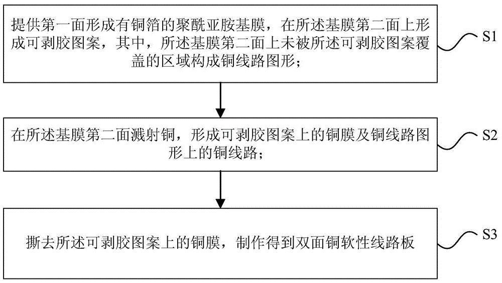
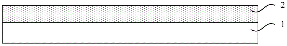
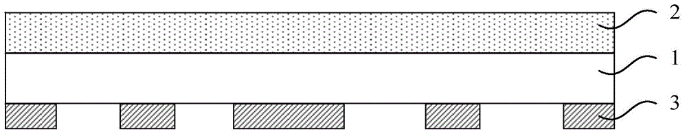
[0039] See Figure 1 to Figure 6 . It should be noted that the illustrations provided in this embodiment only illustrate the basic idea of the present invention in a schematic way, and the figures only show the components related to the present invention instead of the number, shape, and shape of the components in actual implementation. For size drawing, the type, quantity, and proportion of each component can be changed at will during act...
PUM
| Property | Measurement | Unit |
|---|---|---|
| thickness | aaaaa | aaaaa |
| thickness | aaaaa | aaaaa |
| thickness | aaaaa | aaaaa |
Abstract
Description
Claims
Application Information