An infrared light-emitting diode with multiple roughened layers
A technology of infrared light emitting and roughening layer, applied in electrical components, circuits, semiconductor devices, etc., can solve problems such as unsatisfactory roughening effect, and achieve the effect of improving external quantum efficiency, increasing light-emitting area, and increasing surface light-emitting area
- Summary
- Abstract
- Description
- Claims
- Application Information
AI Technical Summary
Problems solved by technology
Method used
Image

Examples
Embodiment 1
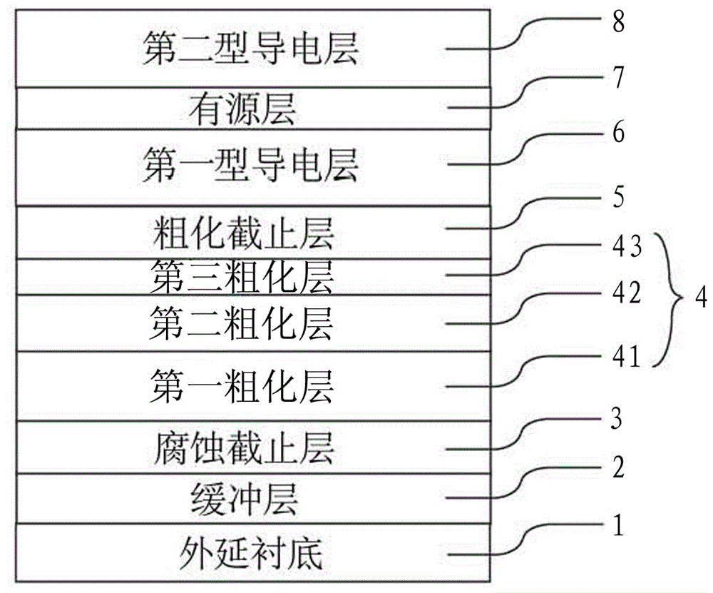
[0051] refer to Figure 1 to Figure 3 As shown, Embodiment 1 of an infrared light-emitting diode with multiple roughened layers disclosed by the present invention, figure 1 It is an epitaxial structure of a near-infrared light-emitting diode, comprising a buffer layer 2, an etching cut-off layer 3, a roughened layer 4, a roughened cut-off layer 5, a first-type conductive layer 6, The active layer 7, the second-type conductive layer 8, and the epitaxial substrate 1 are GaAs substrates.
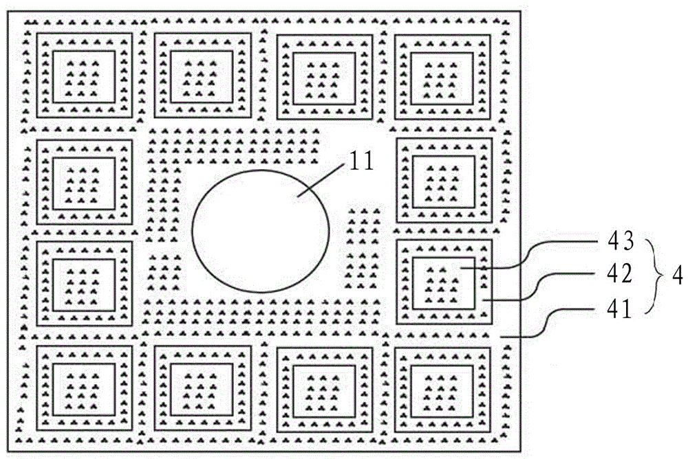
[0052] The roughened layer 4 is composed of a first roughened layer 41 , a second roughened layer 42 and a third roughened layer 43 , the first roughened layer 41 is the outermost roughened layer away from the active layer 7 . The composition material of the roughening layer 4 is AlGaAs, specifically: the first roughening layer 41 is Al 0.3 Ga 0.7 As material, and the thickness of the first roughening layer 41 is 300nm; The second roughening layer 42 is Al 0.5 Ga 0.5 As material, and the t...
Embodiment 2
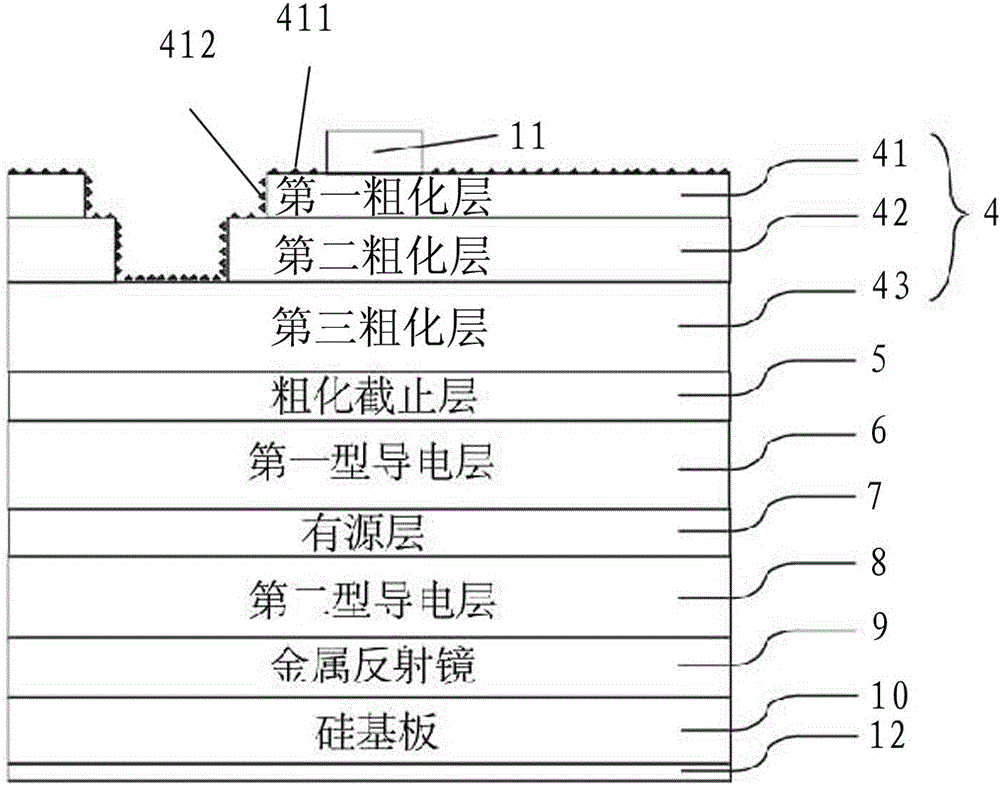
[0067] refer to Figure 4 to Figure 6 As shown, the second embodiment of an infrared light-emitting diode with multiple roughened layers disclosed by the present invention, Figure 4 It is an epitaxial structure of a near-infrared light-emitting diode, including a buffer layer 2, an etching cut-off layer 3, a roughened layer 4, a roughened cut-off layer 5, and a first-type conductive layer 6 sequentially formed on the upper surface of an epitaxial substrate 1 from bottom to top. , an active layer 7, a second-type conductive layer 8, and the epitaxial substrate 1 is a GaAs substrate.
[0068] The roughening layer 4 is made of the first roughening layer 41, the second roughening layer 42, the third roughening layer 43, the fourth roughening layer 44, and the fifth roughening layer 45. The first roughening layer 41 is away from the The outermost roughening layer of the source layer 7. The composition material of the roughening layer 4 is AlGaAs, wherein the material of the firs...
PUM
 Abstract
Description
Claims
Application Information
 - R&D
- Intellectual Property
- Life Sciences
- Materials
- Tech Scout
- Unparalleled Data Quality
- Higher Quality Content
- 60% Fewer Hallucinations
Browse by: Latest US Patents, China's latest patents, Technical Efficacy Thesaurus, Application Domain, Technology Topic, Popular Technical Reports.
© 2025 PatSnap. All rights reserved.Legal|Privacy policy|Modern Slavery Act Transparency Statement|Sitemap|About US| Contact US: help@patsnap.com