

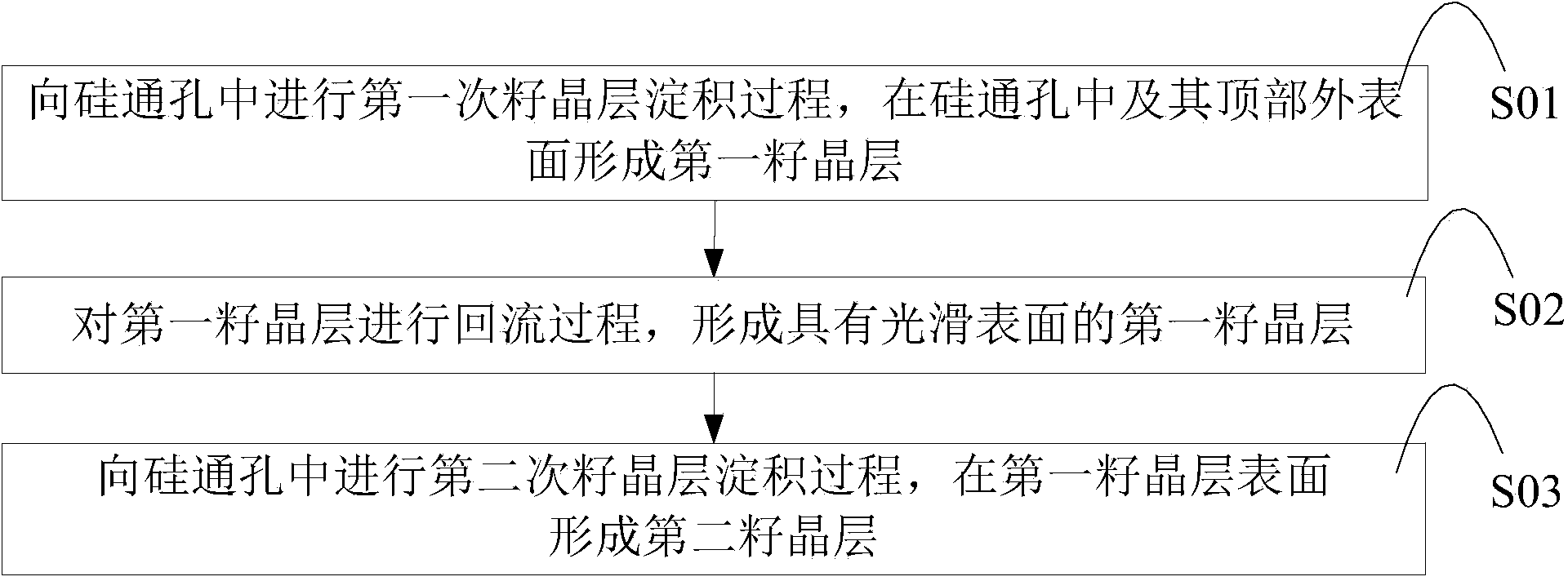
Method for forming seed crystal layers in silicon through hole technology
A technology of seed crystal layer and through-silicon vias, which is applied in the direction of electrical components, semiconductor/solid-state device manufacturing, circuits, etc., can solve problems such as discontinuity, internal void defects in copper, and rough side walls of through-silicon vias, so as to improve reliability. The effect of avoiding void defects
- Summary
- Abstract
- Description
- Claims
- Application Information
AI Technical Summary
Problems solved by technology
Method used
Image

Examples
Embodiment Construction
[0025] In order to make the content of the present invention clearer and easier to understand, the content of the present invention will be further described below in conjunction with the accompanying drawings. Of course, the present invention is not limited to this specific embodiment, and general replacements known to those skilled in the art are also covered within the protection scope of the present invention.
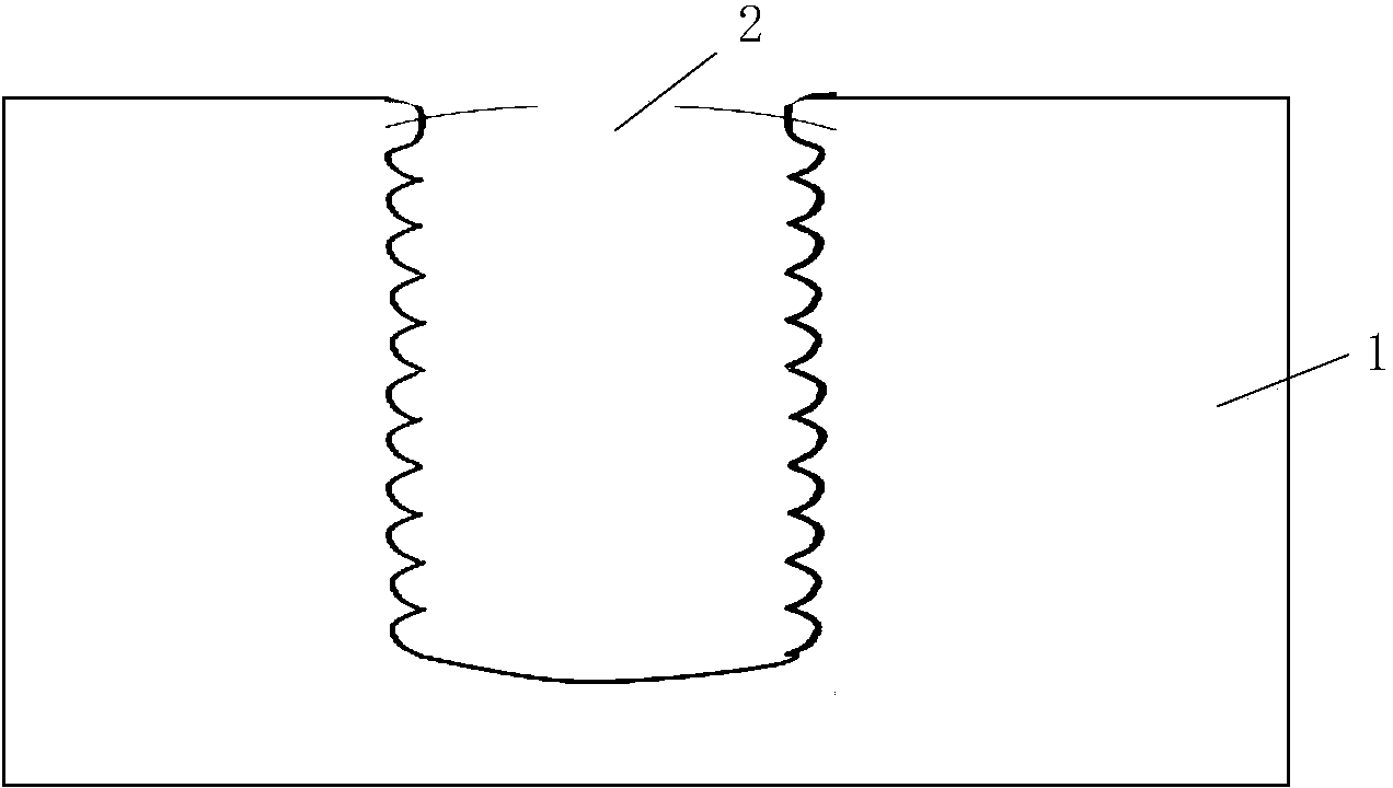
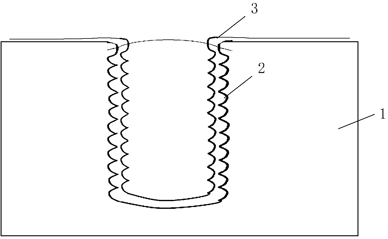
[0026] As mentioned above, in the preparation of through-silicon vias, the smoothness of the deposited seed layer will seriously affect the quality of subsequent copper plating. If the surface of the deposited seed layer is not smooth or discontinuous or at the corner Sharp corners appear at the TSVs, which will cause voids inside the copper filled in the TSVs, seriously affecting the resistance and reliability of the TSVs. Therefore, in order to overcome the above-mentioned defects in the deposition of the existing seed layer, the present invention improves the de...
PUM
 Abstract
Description
Claims
Application Information