Junction barrier Schottky diode
A technology of Schottky diodes and silicon substrates, which is applied in the direction of electrical components, circuits, semiconductor devices, etc., and can solve the problems of increased device size and cost
- Summary
- Abstract
- Description
- Claims
- Application Information
AI Technical Summary
Problems solved by technology
Method used
Image


Examples
Embodiment Construction
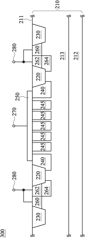
[0048] figure 2 It is a cross-sectional structure diagram of the disclosed first embodiment of the junction barrier Schottky diode 200 of the present invention. The junction barrier Schottky diode 200 of the present invention is a component realized by semiconductor manufacturing process. The junction barrier Schottky diode 200 includes a silicon substrate 210 , a first P-type doped region 240 , a metal layer 250 , a second P-type doped region 262 , and a first N-type doped region 260 .
[0049] The silicon substrate 210 has an upper surface 211 . The silicon substrate 210 has an N-type buried layer 212 below the upper surface 211 . An N-type well 213 is formed between the upper surface 211 of the silicon substrate 210 and the N-type buried layer 212 . The N-type buried layer 212 is used to reduce the leakage current between the upper components, so that the components can be arranged more closely and the overall area can be reduced.
[0050]The first P-type doped region ...
PUM
 Abstract
Description
Claims
Application Information
 - R&D
- Intellectual Property
- Life Sciences
- Materials
- Tech Scout
- Unparalleled Data Quality
- Higher Quality Content
- 60% Fewer Hallucinations
Browse by: Latest US Patents, China's latest patents, Technical Efficacy Thesaurus, Application Domain, Technology Topic, Popular Technical Reports.
© 2025 PatSnap. All rights reserved.Legal|Privacy policy|Modern Slavery Act Transparency Statement|Sitemap|About US| Contact US: help@patsnap.com