Gallium nitride based avalanche detector and preparation method thereof

A gallium nitride-based, manufacturing method technology, applied in semiconductor devices, final product manufacturing, sustainable manufacturing/processing, etc., can solve the problems affecting the development and application of gallium nitride UV detectors, the mutual restriction of detection sensitivity and dark current, etc. question

Inactive Publication Date: 2010-08-25
INST OF SEMICONDUCTORS - CHINESE ACAD OF SCI
View PDF0 Cites 41 Cited by
  • Summary
  • Abstract
  • Description
  • Claims
  • Application Information

AI Technical Summary

Problems solved by technology

However, most of the existing avalanche detectors use absorption and multiplication in the same layer, so the detection sensitivity and

Method used


Image

  • Gallium nitride based avalanche detector and preparation method thereof
  • Gallium nitride based avalanche detector and preparation method thereof
  • Gallium nitride based avalanche detector and preparation method thereof

Examples


Embodiment Construction

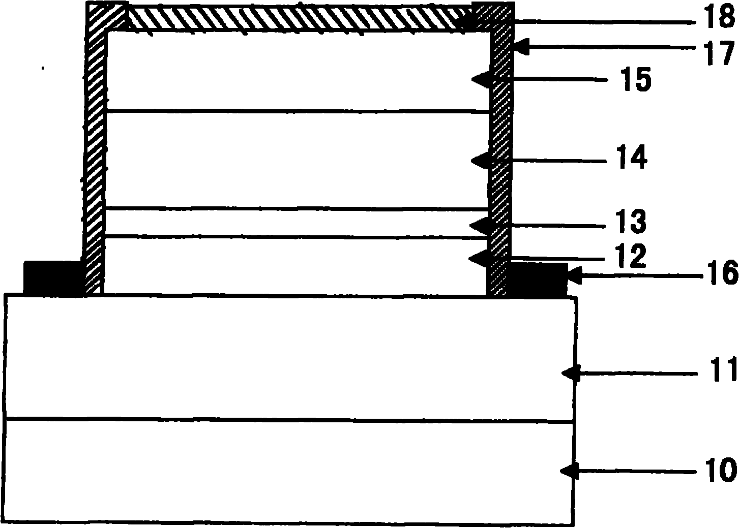
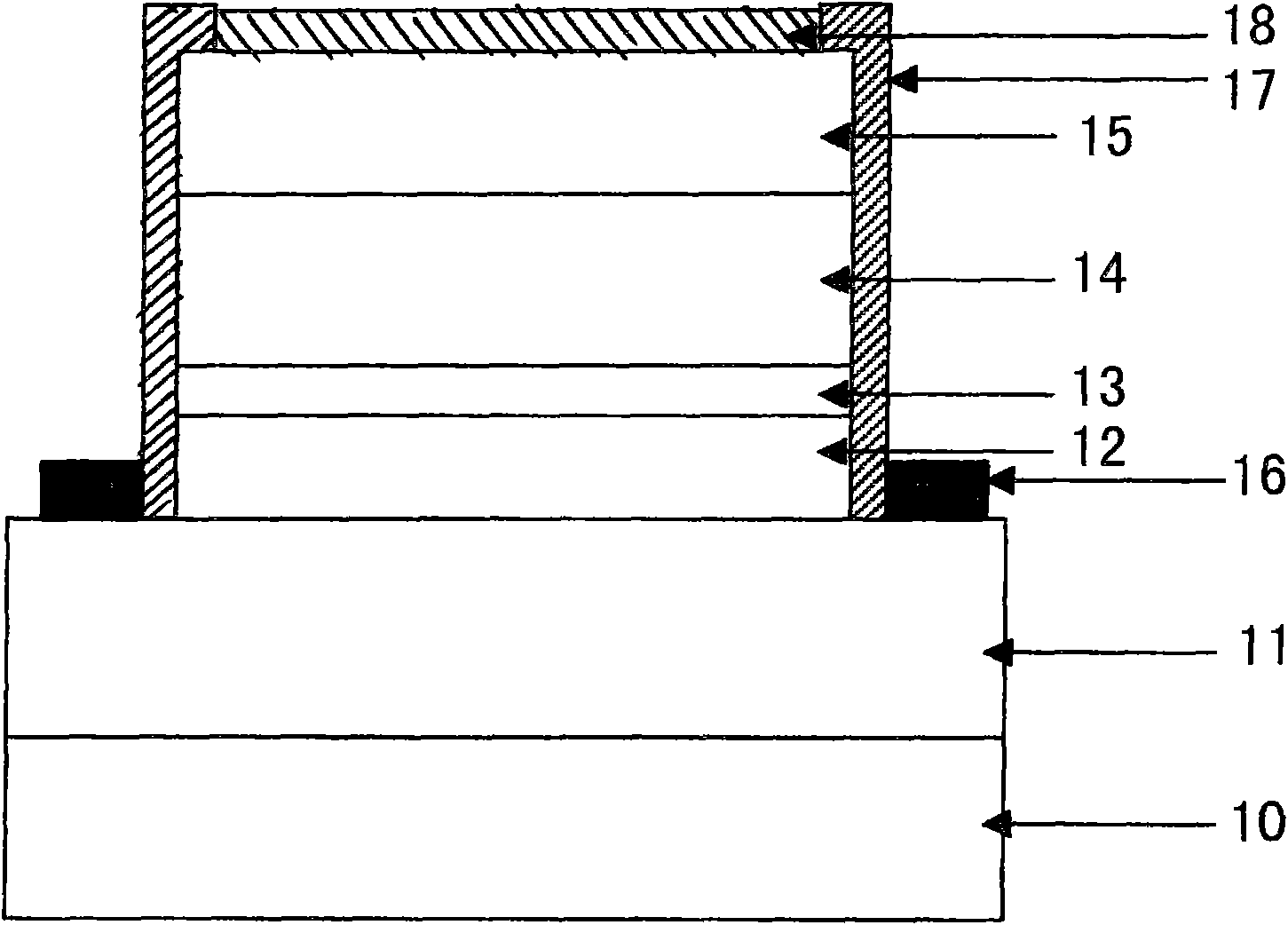
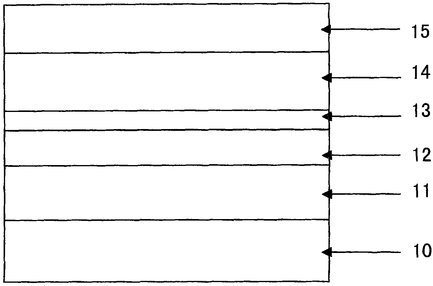
[0042] Please refer to Fig. 1 and Fig. 2, a gallium nitride-based avalanche detector with a positively irradiated absorbing layer and a multiplication layer separated by the present invention includes:

[0043] A substrate 10, the substrate 10 is sapphire, gallium nitride, silicon, silicon carbide or gallium arsenide material which is conducive to the epitaxial growth of group III nitrides;

[0044] An N-type doped GaN ohmic contact layer 11, the N-type doped GaN ohmic contact layer 11 is fabricated on the substrate 10;

[0045] An unintentionally doped GaN absorbing layer 12, the unintentionally doped GaN absorbing layer 12 is made on the N-type doped GaN ohmic contact layer 11, and the area of ​​the unintentionally doped GaN absorbing layer 12 is smaller than that of the N-type doped The area of ​​the GaN ohmic contact layer 11. This layer acts as an absorbing layer for light in the detector response band (photon energy is between the band gaps of GaN and AlGaN);

[0046] ...


PUM


Abstract

The invention relates to a gallium nitride based avalanche detector and a preparation method thereof. The gallium nitride based avalanche detector comprises a substrate, an N-type doped GaN ohmic contact layer, an unintentional doped GaN absorbing layer, an N-type doped Al component gradual changed AlGaN layer, an unintentional doped AlGaN avalanche multiplying layer, a P-type doped AlGaN ohmic contact layer, an N-type ohmic contact electrode and a P-type ohmic contact electrode, wherein the N-type doped GaN ohmic contact layer is prepared on the substrate; the unintentional doped GaN absorbing layer is prepared on the N-type doped GaN ohmic contact layer, and the area of the unintentional doped GaN absorbing layer is smaller than that of the N-type doped GaN ohmic contact layer; the N-type doped Al component gradual changed AlGaN layer is prepared on the unintentional doped GaN absorbing layer; the unintentional doped AlGaN avalanche multiplying layer is prepared on the N-type doped Al component gradual changed AlGaN layer; the P-type doped AlGaN ohmic contact layer is prepared on the unintentional doped AlGaN avalanche multiplying layer; the N-type ohmic contact electrode is prepared on the N-type doped GaN ohmic contact layer; and the P-type ohmic contact electrode is prepared on the P-type doped AlGaN ohmic contact layer.

Description

technical field [0001] The invention belongs to the field of semiconductor devices, in particular the structure and manufacturing method of a novel GaN-based avalanche detector. Background technique [0002] As a third-generation semiconductor, gallium nitride (GaN) and its series of materials (including aluminum nitride, aluminum gallium nitride, indium gallium nitride, and indium nitride) are characterized by their large band gap and wide spectral range (covering from ultraviolet to Infrared full band), high temperature resistance and corrosion resistance, it has great application value in the field of optoelectronics and microelectronics. GaN-based ultraviolet detector is a very important GaN-based optoelectronic device, which is widely used in civil and military fields such as missile early warning, rocket plume detection, ultraviolet communication, biochemical weapon detection, aircraft guidance, spacecraft, ozone layer hole detection, fire monitoring, etc. important a...

Claims


Application Information

Patent Timeline
IPC IPC(8): H01L31/0352H01L31/107H01L31/20
CPCY02P70/50
Inventor 刘文宝孙苋赵德刚刘宗顺张书明朱建军王辉杨辉
Owner INST OF SEMICONDUCTORS - CHINESE ACAD OF SCI
Why Eureka
Try Eureka