
Light emitting diode with enhanced quantum efficiency and method of fabrication

a light-emitting diode and quantum efficiency technology, applied in the direction of diodes, crystal growth process, polycrystalline material growth, etc., can solve the problem of large energy loss

Inactive Publication Date: 2012-09-20
APPLIED MATERIALS INC
View PDF0 Cites 40 Cited by
  • Summary
  • Abstract
  • Description
  • Claims
  • Application Information

AI Technical Summary

Benefits of technology

[0110]In accordance with an embodiment of the present invention, an advantage possibly unique to gallium is exploited, where gallium is a common source metal used in HVPE process formation of group III-nitride materials. In an embodiment, gallium is used to form a eutectic mixture for an HVPE source. Gallium may be used to form a eutectic with almost every element of periodic table, with very rare exceptions. For example, FIG. 20 illustrates, in a periodic table format 2000, a variety of gallium binary systems, in accordance with an embodiment of the present invention. In one embodiment, by forming such eutectics, a variety of dopants available for HVPE processes is broadened significantly. In an embodiment, the overall cost of an HVPE process is lowered by using a eutectic as a metal source, as compared with using metal-organic compound precursors. In one embodiment, the specific composition of a eutectic mixture for HVPE is selected by consulting temperature-composition phase diagrams of binary compounds.

Problems solved by technology

These two processes are accompanied by large energy losses, which are attributed to high temperatures and large Stokes shift characteristics.

Method used


Image

  • Light emitting diode with enhanced quantum efficiency and method of fabrication
  • Light emitting diode with enhanced quantum efficiency and method of fabrication
  • Light emitting diode with enhanced quantum efficiency and method of fabrication

Examples


Embodiment Construction

[0042]In the following description, numerous specific details are set forth, such as fabrication conditions and material regimes, in order to provide a thorough understanding of embodiments of the present invention. It will be apparent to one skilled in the art that embodiments of the present invention may be practiced without these specific details. In other instances, well-known features, such as facility layouts or specific tool configurations, are not described in detail in order to not unnecessarily obscure embodiments of the present invention. Furthermore, it is to be understood that the various embodiments shown in the Figures are illustrative representations and are not necessarily drawn to scale. Additionally, other arrangements and configurations may not be explicitly disclosed in embodiments herein, but are still considered to be within the spirit and scope of the invention.

[0043]Embodiments of the present invention, improve the quantum efficiency of III-V compound semico...


PUM

PropertyMeasurementUnit
Volumeaaaaaaaaaa
Volumeaaaaaaaaaa
Volumeaaaaaaaaaa

Abstract

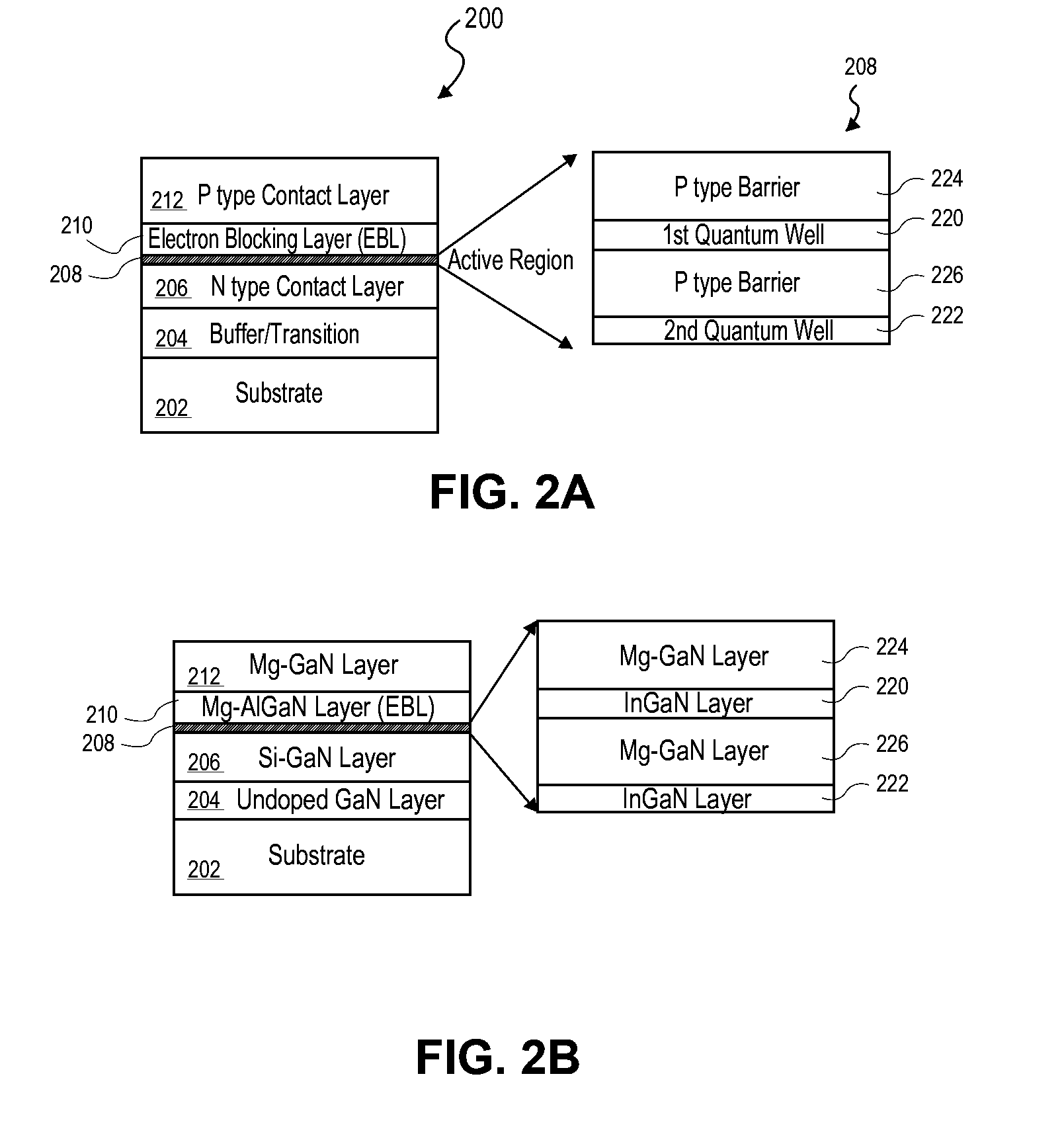
One embodiment of a quantum well structure comprises an active region including active layers that comprise quantum wells and barrier layers wherein some or all of the active layers are p type doped. P type doping some or all of the active layers improves the quantum efficiency of III-V compound semiconductor light emitting diodes by locating the position of the P-N junction in the active region of the device thereby enabling the dominant radiative recombination to occur within the active region. In one embodiment, the quantum well structure is fabricated in a cluster tool having a hydride vapor phase epitaxial (HVPE) deposition chamber with a eutectic source alloy. In one embodiment, the indium gallium nitride (InGaN) layer and the magnesium doped gallium nitride (Mg—GaN) or magnesium doped aluminum gallium nitride (Mg—AlGaN) layer are grown in separate chambers by a cluster tool to avoid indium and magnesium cross contamination. Doping of group III-nitrides by hydride vapor phase epitaxy using group III-metal eutectics is also described. In one embodiment, a source is provided for HVPE deposition of a p-type or an n-type group III-nitride epitaxial film, the source including a liquid phase mechanical (eutectic) mixture with a group III species. In one embodiment, a method is provided for performing HVPE deposition of a p-type or an n-type group III-nitride epitaxial film, the method including using a liquid phase mechanical (eutectic) mixture with a group III species.

Description

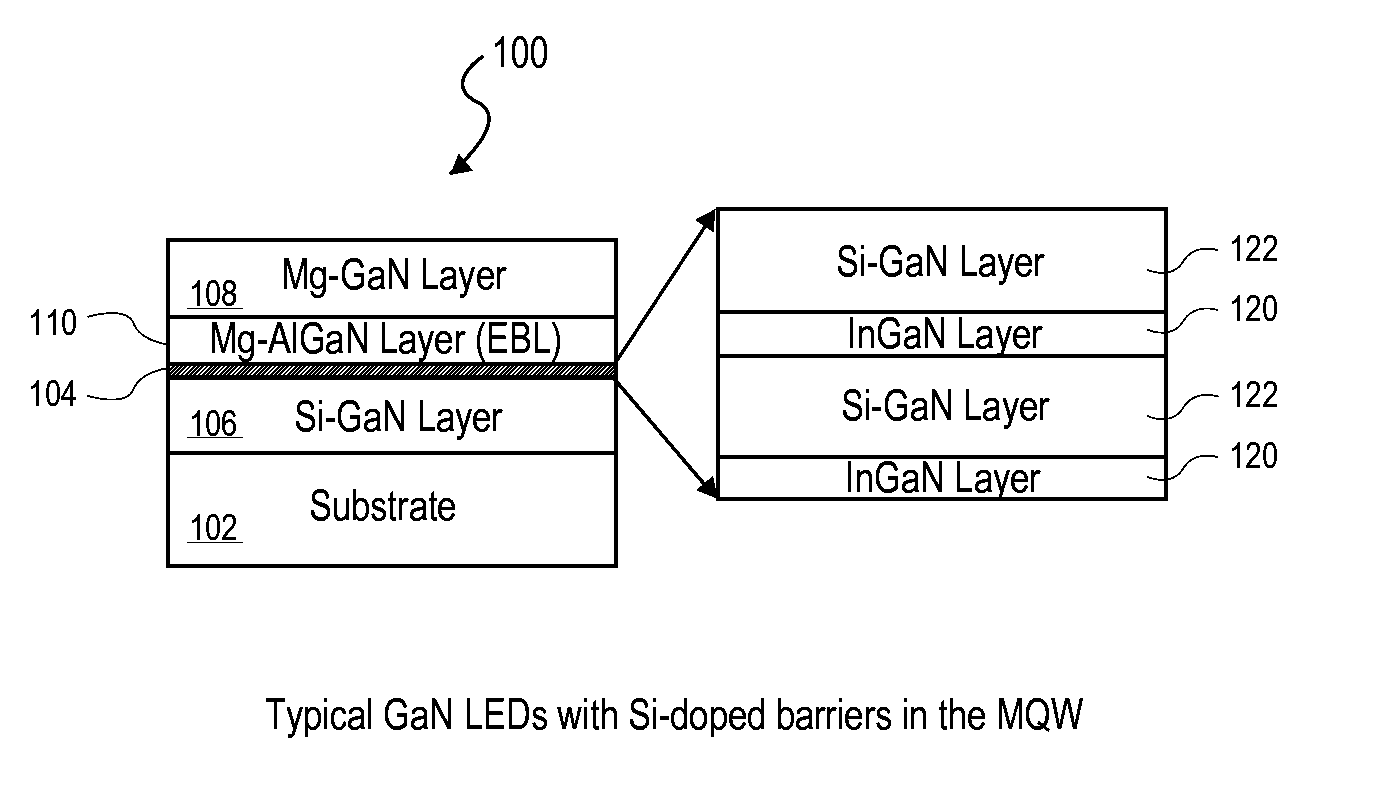
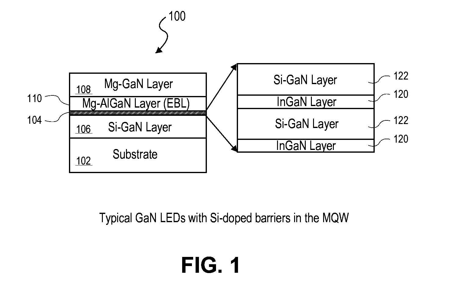
CROSS REFERENCE TO RELATED APPLICATIONS[0001]This application claims the benefit of U.S. Provisional Application No. 61 / 230,438, filed Jul. 31, 2009 and U.S. Provisional Application No. 61 / 263,735, filed Nov. 23, 2009, the entire contents of which are hereby incorporated by reference herein.BACKGROUND[0002]1. Field[0003]Embodiments of the present invention relate to light emitting diodes with enhanced quantum efficiency and their methods of fabrication.[0004]2. Discussion of Related Art[0005]Light emitting diodes (LEDs) are the ultimate light source in lighting technology. The LED technology has flourished for the past few decades. High efficiency, reliability, rugged construction, low power consumption, and durability are among the key factors for the rapid development of the solid-state lighting based on high-brightness visible LEDs. Conventional light sources, such as filament light bulbs or fluorescent lamps depend on either incandescence or discharge in gases. These two process...

Claims


Application Information

Patent Timeline
IPC IPC(8): H01L33/04C30B25/02H01B1/02C30B25/08
CPCH01L33/04H01L33/325H01L33/06
Inventor SU, JIEKRYLIOUK, OLGAMELNIK, YURIYKOJIRI, HIDEHIROCHEN, LUISHIKAWA, TETSUYA
Owner APPLIED MATERIALS INC
Learn More