
Method for measuring and compensating absolute positioning accuracy of precise positioning platform

An absolute positioning accuracy and precise positioning technology, which is applied in the photoplate making process, optics, and instruments of the patterned surface, can solve the problems of high cost, high price, and high environmental requirements, and achieve low cost, easy operation, and measurement accuracy. high effect

Inactive Publication Date: 2014-12-10
HEFEI ADVANTOOLS SEMICON
View PDF3 Cites 29 Cited by
  • Summary
  • Abstract
  • Description
  • Claims
  • Application Information

AI Technical Summary

Problems solved by technology

Using a laser interferometer is expensive. If you only measure and compensate the positioning accuracy of a single axis, you can use a single-axis laser interferometer. If you measure and compensate the positioning accuracy of each position on the two-dimensional plane for the XY integrated platform, you need a length Reflectors that can cover the travel of the XY axis are more expensive than single-axis compensation. This method has high environmental requirements, and requires stable temperature and humidity, cleanliness, etc., and the construction of this measurement system requires a complicated adjustment process.

Method used


Image

  • Method for measuring and compensating absolute positioning accuracy of precise positioning platform
  • Method for measuring and compensating absolute positioning accuracy of precise positioning platform
  • Method for measuring and compensating absolute positioning accuracy of precise positioning platform

Examples


Embodiment Construction

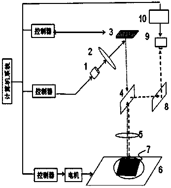
[0028] like figure 1 As shown, the hardware system of the direct writing lithography equipment includes an exposure light source 1, a spatial light modulator 3, a substrate 7 installed on a mobile platform 6, the mobile platform 6 is connected to a motor, the motor is connected to a platform controller, the exposure light source 1, the spatial light modulator An optical integration system 2 is installed between the modulators 3, an inclined beam splitter 4 and a lens or lens group 5 are arranged between the spatial light modulator 3 and the substrate 6, and the reflected light of the beam splitter 4 enters the CCD in the imaging module Camera 9, CCD camera 9 is connected with image processing module 10.

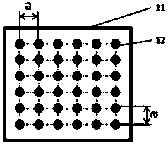
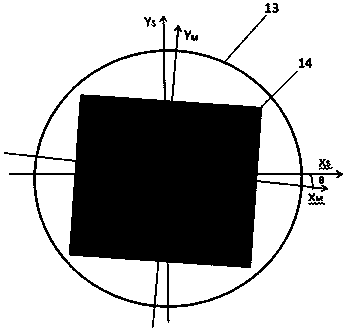
[0029] like Figure 2-6 As shown, a method for measuring and compensating the absolute positioning accuracy of a precision positioning platform includes the following steps:

[0030] 1. If figure 2 As shown, the mask plate 11 is fixed on the sucker of a lithography equip...


PUM


Abstract

The invention discloses a method for measuring and compensating absolute positioning accuracy of a precise positioning platform. The method comprises the following specific steps: putting a mask plate on a photo-etching device with high known positioning accuracy, exposing a plurality of regularly arranged Marks on the photo-etching device, measuring a positioning platform with poor accuracy by virtue of the mark plate, a CCD imaging technology and an image matching technology after etching, and compensating a measured error to a platform controller so as to improve the positioning accuracy of the platform. The method is used for measuring and compensating the error by exposing the marks on the mask plate; compared with a method of measurement and compensation with a laser interferometer in the prior art, the method is low in cost and easy to operate; when the image matching method is used for measuring and compensating, the measurement accuracy is high, and the error is 1 / 20 pixel, namely 4.65 microns / 22.3 / 20 which is about 10nm; the method is capable of effectively compensating and calibrating the two-dimensional positioning accuracy of the positioning platform.

Description

technical field [0001] The invention belongs to the technical field of plate-making lithography, and relates to an absolute positioning accuracy measurement and compensation method of a precision positioning platform on plate-making lithography equipment. Background technique [0002] Photolithography is used to print a pattern of features on the surface of a substrate. Such substrates may include chips used in the manufacture of semiconductor devices, various integrated circuits, flat panel displays (eg, liquid crystal displays), circuit boards, biochips, micromechanical electronic chips, optoelectronic circuit chips, and the like. [0003] The process of lithography plate making is: place the mask or wafer on the precision positioning platform system, use vacuum adsorption, and project the designed characteristic pattern onto the surface of the mask through the exposure device in the lithography equipment. The graphics on the mask plate are as consistent as possible with ...

Claims


Application Information

Patent Timeline
Patent Type & Authority Applications(China)
IPC IPC(8): G03F7/20G03F9/00
Inventor 李香滨
Owner HEFEI ADVANTOOLS SEMICON
Learn More