Multilayer printing technology based waveguide and preparation method thereof

A multi-layer printing and waveguide technology, applied in the directions of waveguides, waveguide-type devices, printed circuit components, etc., can solve the problems of high process requirements, difficult integration of metal waveguides, and difficulty in implementation, saving metal resources, avoiding Mechanical connection problems, the effect of simplified processing

Active Publication Date: 2014-12-17
XIAN INSTITUE OF SPACE RADIO TECH
View PDF9 Cites 5 Cited by
  • Summary
  • Abstract
  • Description
  • Claims
  • Application Information

AI Technical Summary

Problems solved by technology

[0003] The metal waveguide adopts a three-dimensional structure, and its transmission loss is smaller than that of a planar structure waveguide. Generally, the transmission loss of a metal structure waveguide is about one-tenth of the SIW transmission loss. The process requirements are high, and the realization is difficult, especially the connection between structural parts and planar circuits, which has always been a difficulty in the integration of metal waveguides

Method used


Image

  • Multilayer printing technology based waveguide and preparation method thereof
  • Multilayer printing technology based waveguide and preparation method thereof
  • Multilayer printing technology based waveguide and preparation method thereof

Examples


preparation example Construction

[0036] The above-mentioned method for preparing a waveguide based on multi-layer printing technology includes the following steps:

[0037](1), set the broadside length a and height b of the metal waveguide;

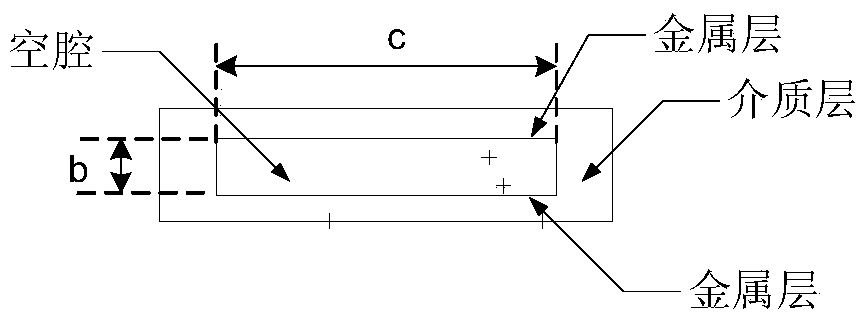
[0038] (2) Select m-layer flat printed boards as the dielectric substrate group, wherein m is a positive integer and m≥3; the m-layer flat printed boards are sorted from top to bottom as the first layer to the mth layer, wherein the first The total thickness of the planar printed boards from the 2nd layer to the m-1th layer is equal to the height b of the metal waveguide set in the step (1);

[0039] (3), metal coating is carried out on the lower surface of the first layer of flat printed board and the upper surface of the mth layer of flat printed board;

[0040] (4), adopt multi-layer PCB or LTCC process to process the flat printed board of the 2nd layer~m-1 layer, form a cavity between the two layers of metal coating layers obtained in step (3), The length of the na...

Embodiment

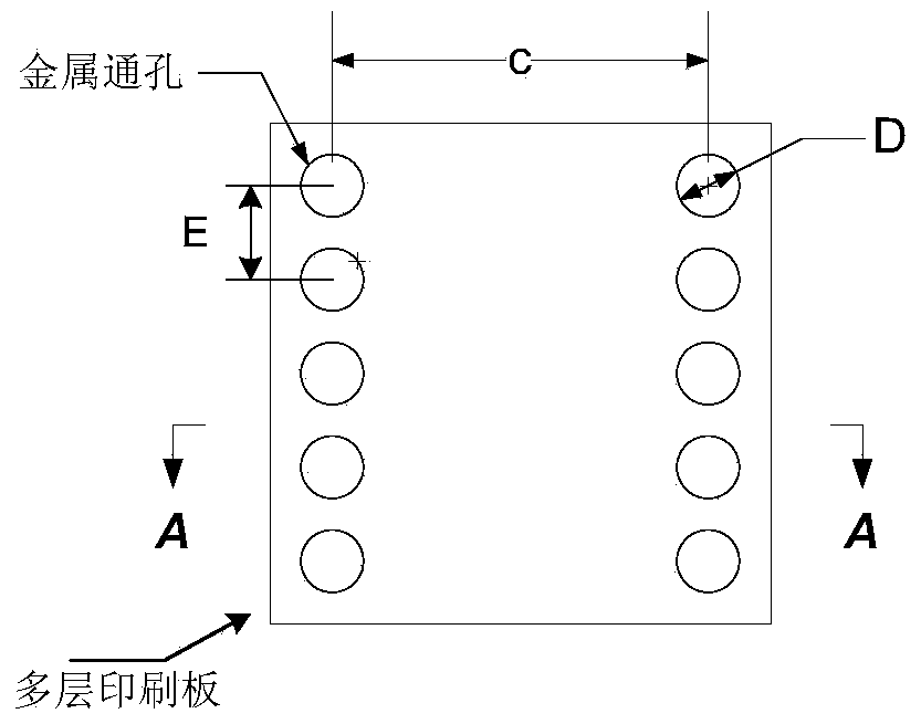
[0047] The working center frequency of the waveguide is f=14GHz, and m-layer flat printed boards are used as the dielectric substrate group. Among them, the total thickness of the flat printed boards from the second layer to the m-1th layer is 7mm, and the lower surface of the first layer of flat printed boards and There is a metal coating layer on the upper surface of the mth layer of the flat printing plate, and the thickness of the metal coating layer is 7um; the length of the narrow side of the cavity between the two metal coating layers is 7mm, and the length c of the wide side is 14mm; Metal through-holes are provided on the surface of the board, and the metal through-holes pass through the m-layer planar printing plate, and the metal through-holes are distributed in two rows in parallel on the surface of the planar printing plate, and the distribution direction is perpendicular to the width direction of the cavity , wherein the diameter of the metal vias D=0.4mm, the cen...


PUM


Abstract

The invention relates to a multilayer printing technology based waveguide and a preparation method thereof. The multilayer printing technology based waveguide is characterized in that multiplayer surface plates serve as a dielectric substrate group, the top surface plate and the bottom surface plate are subjected to metal coating, and a cavity and metal holes are formed in the dielectric substrate group consisting of the multiplayer surface plates according to design, so that a substrate integrated metal waveguide is obtained. The multilayer printing technology based waveguide follows a method that SIW (substrate integrated waveguide) discrete grounding substitutes for continuous grounding, and a metalloid waveguide structure is achieved in a multilayer printing structure. The substrate integrated metal waveguide obtained by the preparation method according to the design is consistent with a metal waveguide in transmission characteristic when radiation loss is neglected, and a waveguide processing technique is simplified.

Description

technical field [0001] The invention relates to the field of microwave transmission lines, in particular to a waveguide based on multilayer printing technology and a preparation method thereof, wherein a planar metal waveguide is obtained by adopting planar multilayer printing and discrete grounding treatment design. Background technique [0002] Substrate-integrated waveguide (SIW) is a microwave integration technology that has become popular in the world in recent years, and has attracted great attention from the academic community. In the microwave high-frequency band, SIW can obtain a higher single-cavity unloaded Q value compared with ordinary planar circuits. The highest unloaded Q value of ordinary planar circuits is about 100, while the unloaded Q value of SIW can be as high as 300~ 500, so SIW is used to transmit microwave signals, and its insertion loss is about half of that of planar waveguides, so it has been widely used. [0003] The metal waveguide adopts a th...

Claims


Application Information

Patent Timeline
Patent Type & Authority Applications(China)
IPC IPC(8): H01P3/12H05K1/02
Inventor 禹旭敏杨毅民林浩佳李秋强杨军
Owner XIAN INSTITUE OF SPACE RADIO TECH
Why Eureka
Try Eureka