Circuit board and manufacture method thereof

A circuit board production and circuit board technology, which is applied in the directions of printed circuit components, electrical connection printed components, and the formation of printed component electrical connections, can solve the problem of unfavorable dense arrangement of conductive lines and cannot meet the needs of dense conductive lines on circuit boards Requirements and other issues, to achieve the effect of dense line distribution

Inactive Publication Date: 2014-12-17
QI DING TECHNOLOGY QINHUANGDAO CO LTD +1
View PDF5 Cites 13 Cited by
  • Summary
  • Abstract
  • Description
  • Claims
  • Application Information

AI Technical Summary

Problems solved by technology

Due to the existence of the annular ring, it is not conducive to the dense arrangement of conductive lines, and cannot meet the requirements of dense conductive lines on the circuit board

Method used


Image

  • Circuit board and manufacture method thereof
  • Circuit board and manufacture method thereof
  • Circuit board and manufacture method thereof

Examples


Embodiment Construction

[0021] The circuit board manufacturing method provided by the technical solution includes the following steps:

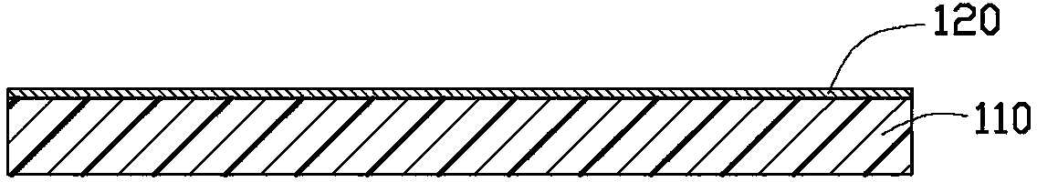
[0022] For a first step, see figure 1 , providing the carrier 110 and the first copper foil 120 .

[0023] The carrier 110 is used to support the first copper foil 120 . The first copper foil 120 is a thin copper foil, and the thickness of the first copper foil 120 is 2 microns to 5 microns. The carrier 110 is made of a metal material different from that of the first copper foil 120 or made of a non-metal material. The metal carrier 110 has sufficient mechanical strength to support the first copper foil 120 .

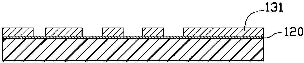
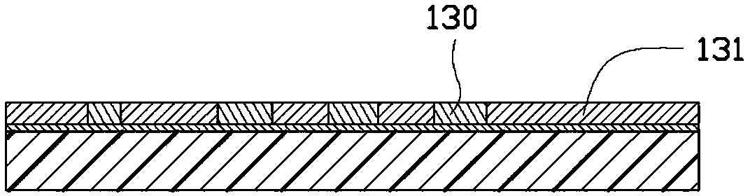
[0024] In the second step, please also refer to the Figure 2 to Figure 4 , forming the first conductive circuit layer 130 on the surface of the first copper foil 120 .

[0025] The formation of the first conductive circuit layer 130 may include the following steps:

[0026] First, a first photoresist pattern layer 131 is formed on the surface of the fi...


PUM


Abstract

The invention discloses a circuit board, comprising a dielectric layer, a first conductive circuit layer and a second conductive circuit layer, wherein the dielectric layer is provided with a first surface and a second surface opposite to each other, at least one first hole is formed from the second surface to the first surface, the first hole is filled with plated metal to form a conductive hole, the first conductive circuit layer is embedded into one side of the first surface of the dielectric layer, the second conductive circuit layer is formed on the second surface of the dielectric layer, at least one conductive circuit in the first conductive circuit layer and the conductive metal in the first hole communicates with each other, and the conductive metal in the first hole is provided with a first end face that is exposed from one side of the first surface. The invention also provides a manufacture method of the circuit board.

Description

technical field [0001] The invention relates to the field of circuit board production, in particular to a circuit board with an electrical connector and a production method thereof. Background technique [0002] During the manufacturing process of the circuit board, it is usually necessary to make conductive blind holes to connect two or more layers of conductive lines. For conductive blind vias, a dielectric layer is usually laminated on a circuit substrate with conductive pads, and a first opening corresponding to the conductive pads is formed by laser ablation. Then a photoresist layer is formed on the dielectric layer, and a second opening corresponding to the first opening is obtained by exposing and developing the photoresist layer. The second opening is formed by means of exposure and development. Due to the requirement of manufacturing equipment, the opening size of the second opening needs to be larger than that of the first opening so as to fully expose the first ...

Claims


Application Information

Patent Timeline
Patent Type & Authority Applications(China)
IPC IPC(8): H05K1/11H05K3/42
Inventor 胡文宏
Owner QI DING TECHNOLOGY QINHUANGDAO CO LTD
Why Eureka
Try Eureka