Wiring board

A technology of wiring substrates and insulating substrates, which is applied to the layout details of conductive patterns, printed circuits, printed circuits connected with non-printed electrical components, etc., can solve problems such as cracks, and achieve the effect of improving joint strength

Inactive Publication Date: 2014-12-17
KYOCERA CORP
View PDF10 Cites 4 Cited by
  • Summary
  • Abstract
  • Description
  • Claims
  • Application Information

AI Technical Summary

Problems solved by technology

Therefore, cracks are likely to occur on the bonding surface between the first via-hole conductor 30a and the lower layer conductors 26, 26a, and sometimes the first semiconductor element S1 cannot be stably operated.

Method used


Image

  • Wiring board
  • Wiring board
  • Wiring board

Examples


Embodiment Construction

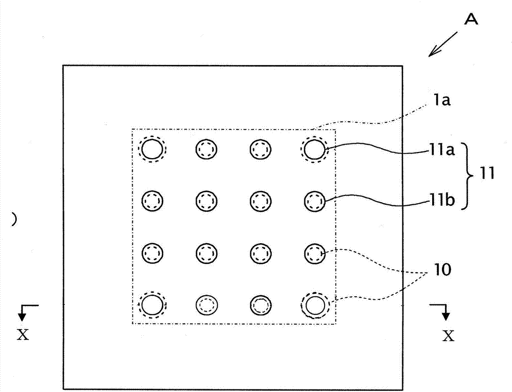
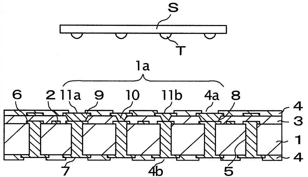
[0043] Next, an embodiment of a wiring board in the first aspect of the present invention will be described based on FIG. 1 . Figure 1A is a schematic plan view of the wiring board A, Figure 1B yes Figure 1A XX-line side cross-sectional view. Such as Figure 1B As shown, the wiring board A includes an insulating substrate 1 , a wiring conductor 2 , an insulating layer 3 , and a solder resist layer 4 . In the central portion of the upper surface of the wiring board A, for example, a semiconductor element mounting portion 1 a for mounting a large semiconductor element S for arithmetic processing or the like is formed in a quadrangular shape.

[0044] The insulating substrate 1 is made of, for example, glass-epoxy resin. A plurality of through holes 5 penetrating from the upper surface toward the lower surface are formed in the insulating substrate 1 . Part of the wiring conductor 2 is covered on the upper and lower surfaces of the insulating substrate 1 and the inside of...


PUM


Abstract

A wiring board according to the present invention includes an insulating layer 3, a semiconductor element mounting portion 1a, semiconductor element connection pads 11, via holes 8, and via conductors 10. The semiconductor element connection pads 11 aligned on the semiconductor element mounting portion 1a include first semiconductor element connection pads 11a and other second semiconductor element connection pads 11b, and the diameters of the via conductors 10 connected to the first semiconductor element connection pads 11a are larger than the diameters of the via conductors 10 connected to the second semiconductor element connection pads 11b.

Description

technical field [0001] The present invention relates to a wiring board for mounting semiconductor elements and the like. Background technique [0002] In recent years, electronic devices represented by mobile phones, music players, and the like have been increasingly enhanced in functionality. High-performance large-scale semiconductor elements for arithmetic processing and the like are sometimes mounted on the wiring boards used for them. [0003] FIG. 15 shows a conventional wiring board E on which a large semiconductor element is mounted. Figure 15A is a plan view of the wiring substrate E, Figure 15B is through Figure 15A The cross-sectional view between Y-Y. Such as Figure 15B As shown, the wiring substrate E includes an insulating substrate 21 formed with a plurality of through-holes 25 , a wiring conductor 22 , an insulating layer 23 laminated on the upper surface of the insulating substrate 21 , and a solder resist layer 24 . In the central portion of the upp...

Claims


Application Information

Patent Timeline
Patent Type & Authority Applications(China)
IPC IPC(8): H05K1/11H05K1/18H01L23/498
CPCH05K1/113H01L24/81H01L2924/12042H01L2924/351H05K1/0298H05K3/3436H05K2201/094H01L2924/00
Inventor 服部诚司
Owner KYOCERA CORP
Why Eureka
Try Eureka