Supercharge Your Innovation With Domain-Expert AI Agents!

ITO (indium tin oxide) transparent conductive film

A technology of transparent conductive film and transparent conductive layer, which is applied in the optical field, can solve the problems of obvious etching lines and difficult to completely eliminate etching lines of ITO transparent conductive film, and achieve the effect of eliminating obvious etching lines

Inactive Publication Date: 2014-12-24
ZHANGJIAGANG KANGDE XIN OPTRONICS MATERIAL
View PDF5 Cites 5 Cited by
  • Summary
  • Abstract
  • Description
  • Claims
  • Application Information

AI Technical Summary

Problems solved by technology

[0006] With the rise of high-end large touch screen devices and the front self-luminous application of OLED technology, we require that the etching lines and color difference are not visible, but it is difficult to completely eliminate the etching lines of the ITO transparent conductive film used for Touch Sensor, resulting in the current market Some mobile phones and other devices on the Internet have more obvious etching lines, which are some technical problems now.

Method used


Image

  • ITO (indium tin oxide) transparent conductive film
  • ITO (indium tin oxide) transparent conductive film
  • ITO (indium tin oxide) transparent conductive film

Examples


Embodiment Construction

[0028] The present invention will be described in detail below in conjunction with specific embodiments shown in the accompanying drawings. However, these embodiments do not limit the present invention, and any structural, method, or functional changes made by those skilled in the art according to these embodiments are included in the protection scope of the present invention.

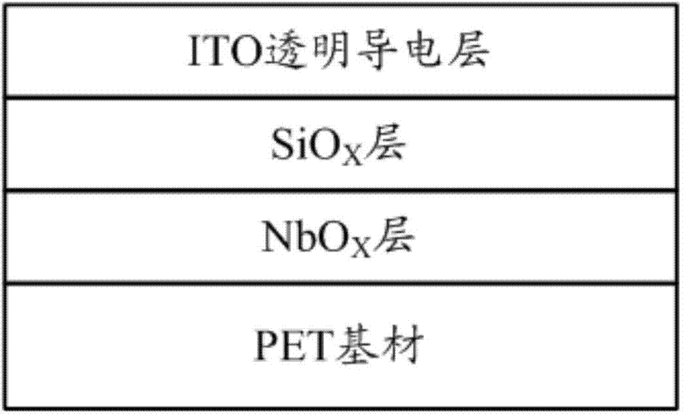
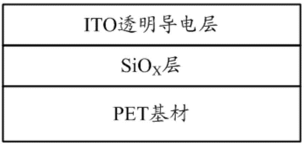
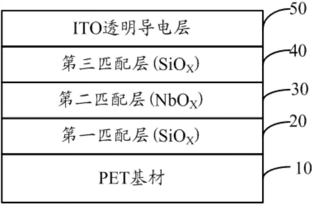
[0029] In the prior art, the production process of ITO transparent conductive film is as follows: a winding vacuum magnetron sputtering coating machine is used as the production equipment, a specific PET film is selected as the substrate, and the specific material is firstly sputtered through the design of the optical film system. A plurality of composite film layers are formed on the surface of the PET film, and then ITO is sputtered onto the material of the composite film layer to form an ITO transparent conductive film with conductive properties.

[0030] In the production process of transparent con...


PUM

PropertyMeasurementUnit
thicknessaaaaaaaaaa
thicknessaaaaaaaaaa
thicknessaaaaaaaaaa

Abstract

The invention discloses an ITO (indium tin oxide) transparent conductive film. The ITO transparent conductive film sequentially comprises a PET (polyethylene terephthalate) base material, a first IM (intensity modulation) layer, a second IM layer and an ITO transparent conductive layer, wherein the first IM layer comprises a HC (hydrocarbon compound) hardening layer and a first matching layer; the HC hardening layer is coated on the PET base material; the first matching layer is positioned on the HC hardening layer; the refractive index of the first matching layer is greater than that of the HC hardening layer; the refractive index of the first matching layer is 1.46-1.49; the first matching layer and the HC hardening layer are a high-refractive-index matching layer and a low-refractive-index matching layer respectively; the second IM layer comprises a second matching layer and a third matching layer; the second matching layer and the third matching layer are positioned on the first IM layer; the refractive index of the second matching layer is greater than that of the first matching layer; the refractive index of the second matching layer is 2.2-2.4; the refractive index of the third matching layer is smaller than that of the second matching layer; the refractive index of the third matching layer is 1.46-1.49; and the second matching layer and the third matching layer are a high-refractive-index matching layer and a low-refractive-index matching layer respectively. By double-refractive-index matching and a novel compensation technology, the problem that ITO transparent conductive film products have obvious etching grains can be greatly solved.

Description

technical field [0001] The invention relates to the field of optical technology, in particular to an ITO transparent conductive film. Background technique [0002] The touch screen is composed of a backlight module, a Touch Sensor (touch sensor) and a glass cover. At present, the mainstream Touch Sensor structure on the market is: G+2F, that is, there are two transparent conductive films on the glass, and the two transparent conductive films are made of PET film sputtered IM layer and ITO layer; the two transparent conductive films The ITO surface has been etched to form the x and y matrix patterns of ITO respectively. Capacitance is formed between the x and y matrices. When a finger touches the glass cover, it will affect the capacitance of the contact point. This impact signal passes through the Touch The wires on the Sensor are passed to the IC part of the electronic device, thereby locating the position of the touch point. [0003] The optical performance of the Touch ...

Claims


Application Information

Patent Timeline
Patent Type & Authority Applications(China)
IPC IPC(8): H01B5/14
Inventor 于甄耿佳丁晓峰柯荣峰
Owner ZHANGJIAGANG KANGDE XIN OPTRONICS MATERIAL
Features
  • R&D
  • Intellectual Property
  • Life Sciences
  • Materials
  • Tech Scout
  • Unparalleled Data Quality
  • Higher Quality Content
  • 60% Fewer Hallucinations
Learn More