Semiconductor element structure and manufacturing method thereof

A manufacturing method and semiconductor technology, applied in semiconductor/solid-state device manufacturing, semiconductor devices, semiconductor/solid-state device components, etc., can solve problems such as short circuit of components, failure of contact plug components, and failure of the entire IC, so as to avoid exposure, Effects of Avoiding Metal Gate to Source/Drain Short Circuits

Active Publication Date: 2014-12-24
UNITED MICROELECTRONICS CORP
View PDF4 Cites 10 Cited by
  • Summary
  • Abstract
  • Description
  • Claims
  • Application Information

AI Technical Summary

Problems solved by technology

Under the trend of shrinking width, any alignment error in the manufacture of contact plugs may cause the offset of contact plugs, which may lead to short circuits within or between components
When a contact plug alignment problem occurs within the component, such as between the gate structure and the source/drain, and causes a short circuit, it

Method used


Image

  • Semiconductor element structure and manufacturing method thereof
  • Semiconductor element structure and manufacturing method thereof
  • Semiconductor element structure and manufacturing method thereof

Examples


Embodiment Construction

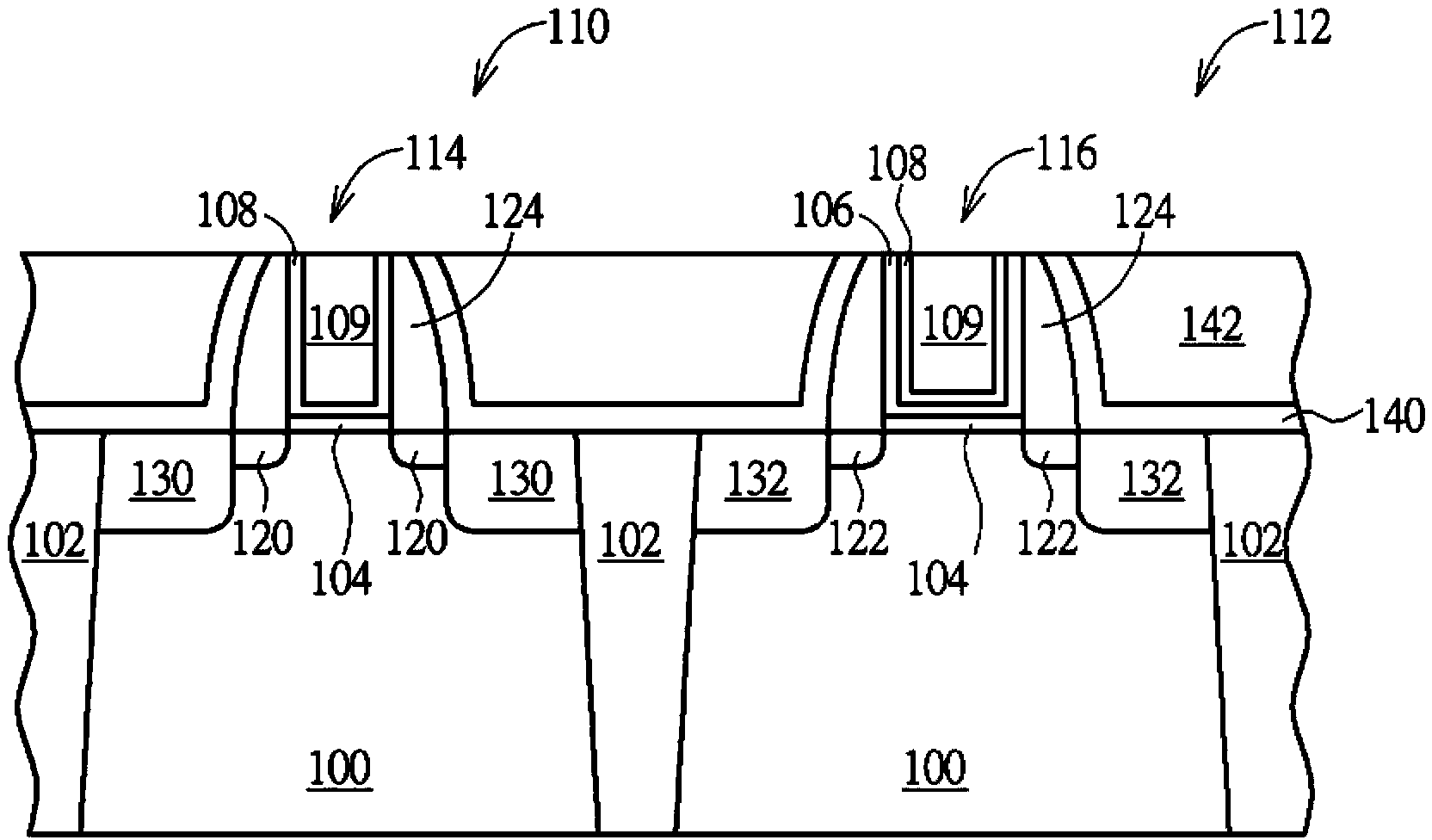
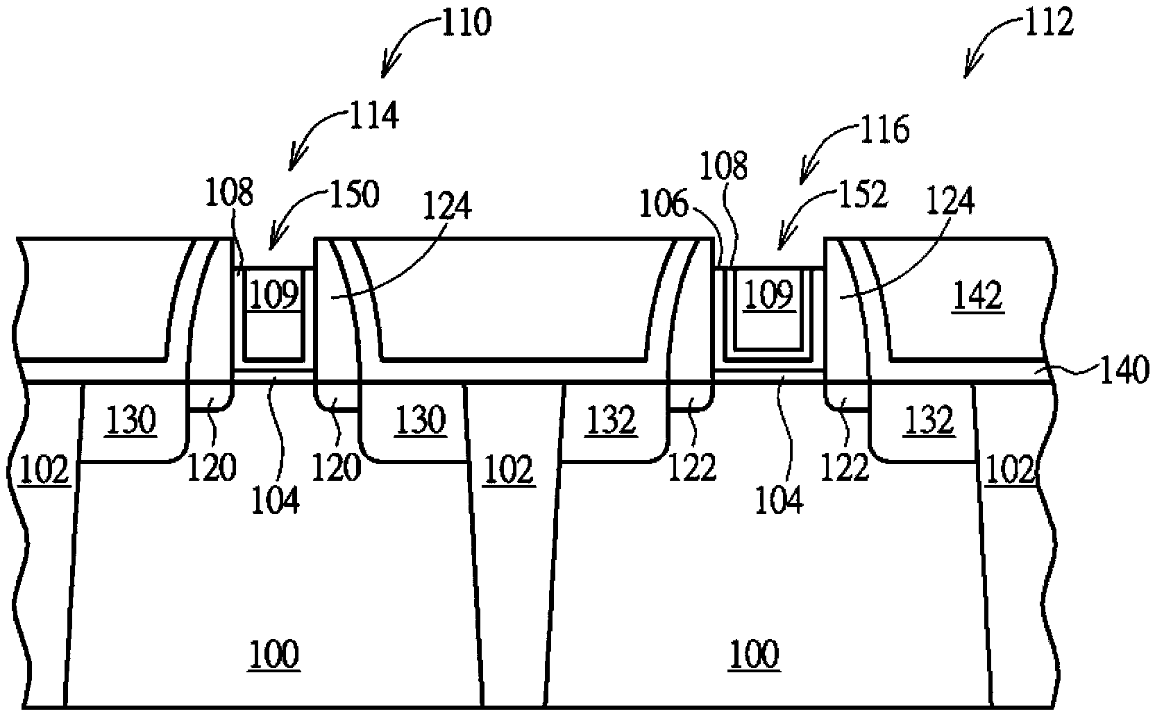
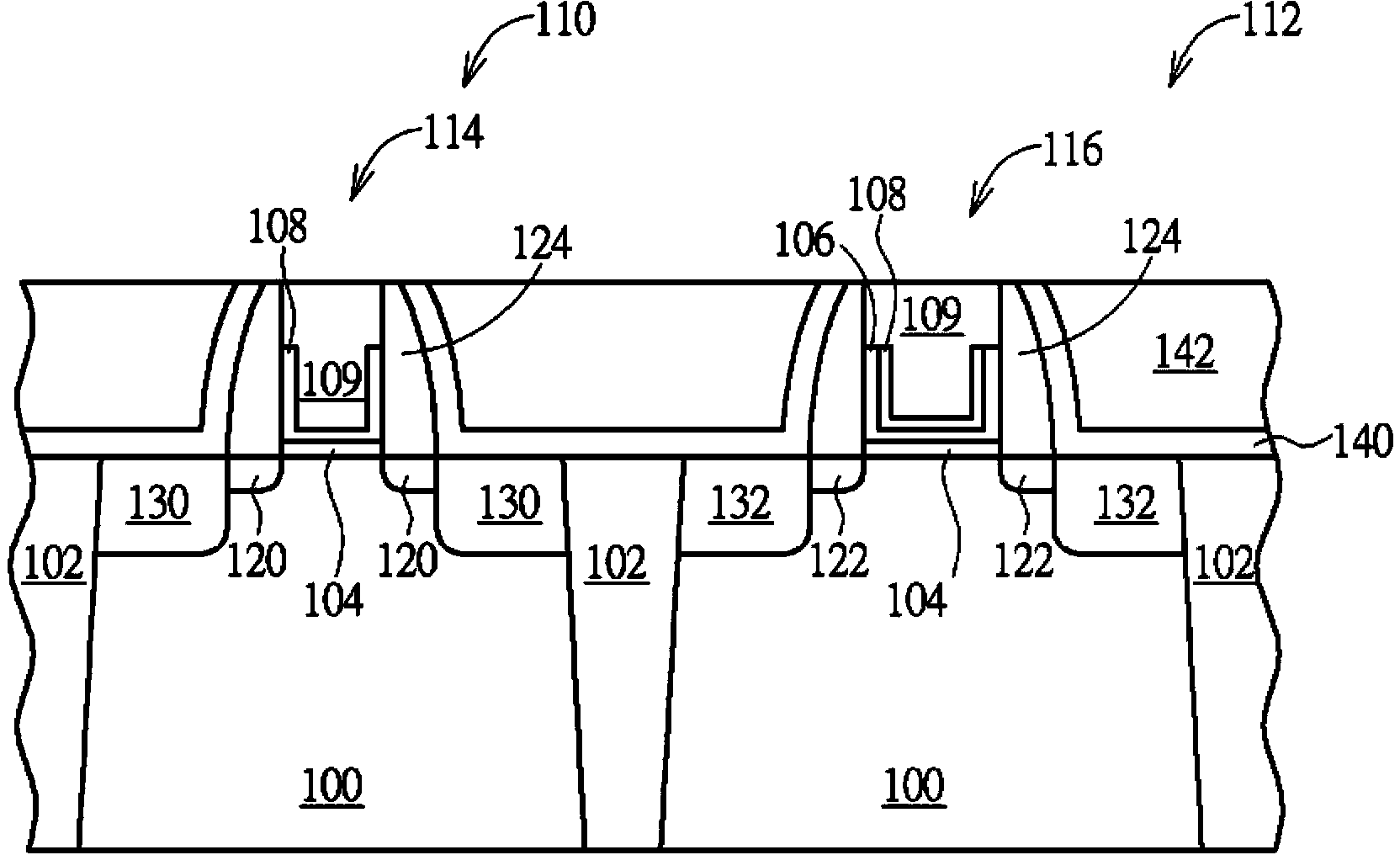
[0045] In order to enable those who are familiar with the technical field of the present invention to further understand the present invention, the preferred embodiments of the present invention are listed below, together with the accompanying drawings, to describe in detail the composition of the present invention and the desired effects .

[0046] For the convenience of description, the drawings of the present invention are only schematic diagrams for easier understanding of the present invention, and the detailed proportions thereof can be adjusted according to design requirements. The upper and lower relationships of the relative components in the figures described in the text should be understood by those skilled in the art to refer to the relative positions of the objects, so all of them can be turned over to present the same components, which should all belong to the disclosure of this specification The scope is described here first.

[0047] see Figure 1 ~ Figure 2 a...


PUM

PropertyMeasurementUnit
Thicknessaaaaaaaaaa

Abstract

The invention discloses a semiconductor element and a manufacturing method of the semiconductor element. The manufacturing method comprises the steps that a substrate is firstly provided, at least one first transistor is formed on the substrate, a first conduction type is included, and the first transistor comprises a first metal grid and a protection layer covering the side wall of the first metal grid; then, part of the first metal grid is removed to form a first groove to expose part of the protection layer, and a second groove is formed by removing the exposed part of the protection layer after the first groove is formed to form. After the second groove is formed, an contact etch stop layer is formed in the second groove.

Description

technical field [0001] The invention relates to a semiconductor structure and a manufacturing method thereof, in particular to a semiconductor element with a metal gate and a contact plug and a manufacturing method thereof. Background technique [0002] In an integrated circuit (IC), various semiconductor elements are electrically connected to each other through contact structures such as contact plugs and interconnection structures. However, as integrated circuits continue to be integrated and feature sizes continue to decrease, the line width and geometric size of semiconductor devices are also getting smaller and smaller. Under the trend of narrowing width, any alignment error in the manufacture of contact plugs may cause offset of the contact plugs, and then lead to short circuits within or between components. When a contact plug alignment problem occurs within the device, such as between the gate structure and the source / drain, and causes a short circuit, it will lead ...

Claims


Application Information

Patent Timeline
IPC IPC(8): H01L29/78H01L29/06H01L21/335
CPCH01L21/76898H01L23/481H01L29/66477H01L29/6653
Inventor 吴宜静黄志森洪庆文
Owner UNITED MICROELECTRONICS CORP
Why Eureka
Try Eureka