A kind of manufacturing method of coreless thin substrate

A manufacturing method and technology for thin substrates, which are applied in the directions of multilayer circuit manufacturing, semiconductor/solid-state device manufacturing, and electrical connection formation of printed components, etc., can solve the problems of increasing the difficulty of circuit thickness control, difficulty in arbitrarily interconnecting circuits, etc., and achieve low cost. , the effect of reducing thickness and reducing process steps

Active Publication Date: 2017-06-30
NAT CENT FOR ADVANCED PACKAGING CO LTD
View PDF3 Cites 0 Cited by
  • Summary
  • Abstract
  • Description
  • Claims
  • Application Information

AI Technical Summary

Problems solved by technology

If the circuit pattern is made first, it is necessary to back-drill or make through holes, and then perform electroplating, which is not easy to realize arbitrary interconnection of the circuit, and increases the difficulty of controlling the thickness of the circuit

Method used


Image

  • A kind of manufacturing method of coreless thin substrate
  • A kind of manufacturing method of coreless thin substrate
  • A kind of manufacturing method of coreless thin substrate

Examples


Embodiment 1

[0042] The manufacturing method of the coreless thin substrate of this embodiment includes the following steps:

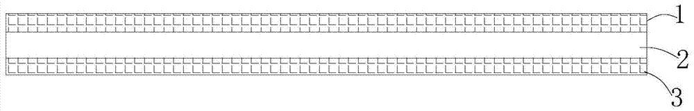
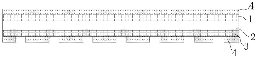
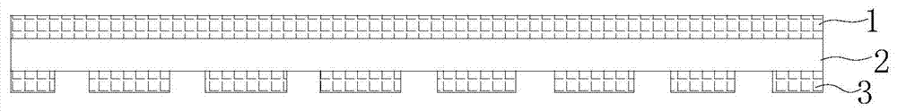
[0043] a. The first copper foil 1, the first prepreg 2, and the second copper foil 3 are stacked sequentially from top to bottom for the first pressing, the first pressing is low-temperature vacuum pressing, and the pressing temperature is the first prepreg The temperature at which the viscosity of 2 is the lowest is preferably 110°C in this embodiment, and is pressed with a vacuum laminating machine under a certain pressure for 15 to 25 minutes, preferably 20 minutes in this embodiment, to obtain the first substrate, such as figure 1 As shown, that is, a double-sided copper-clad prepreg; the first substrate is subjected to dry film pretreatment, such as cleaning or acid treatment, and then the first dry film 4 is pressed on the surface of the first copper foil 1 and the second copper foil 3 respectively, and the The first dry film 4 pressed on the surface of the s...

Embodiment 2

[0050] The difference between this embodiment and Embodiment 1 is that after step d, step e2 replaces step e1, and the third prepreg 14 is respectively pressed on both sides of the substrate model prepared in step d, and the third prepreg 14 is formed by lamination. Multilayer circuits 15 with a specific number of layers are stacked on top to prepare multilayer odd-numbered laminates, such as Figure 15 As shown, the multi-layer circuit is also connected to the first circuit and the third circuit respectively through blind holes. The build-up method used in this embodiment is just a conventional method for making a multi-layer board, and will not be repeated here.


PUM


Abstract

The invention discloses a method for manufacturing a coreless thin substrate, comprising the following steps: a. Laminating first copper foil, first prepreg, and second copper foil sequentially for the first pressing to obtain the first substrate, and Fabricate a second circuit on the second copper foil, the second circuit includes a first pad, and the first pad extends around to form an electroplating frame; b. On the premise that the electroplating frame is exposed, the first pad The second prepreg and the third copper foil are sequentially stacked on the second copper foil and pressed for the second time to obtain the second substrate, and the first circuit and the third circuit are respectively made to obtain the substrate blank; c. The third pressing ; d. Opening the first blind hole and the second blind hole, respectively filling the first blind hole and the second blind hole by using electroplating filling technology to obtain the substrate model. The coreless thin substrate manufactured by the manufacturing method is a three-layer coreless substrate, has symmetrical lamination conditions and lamination structure, and realizes embedding of inner layer circuits.

Description

technical field [0001] The invention relates to the field of substrate processing, in particular to a method for manufacturing a substrate, in particular to a method for manufacturing a coreless thin substrate. Background technique [0002] Coreless substrates (coreless substrates) are currently a hot topic in the development of high-end substrates. Coreless substrates make the package size thinner and smaller, and have a wide range of application prospects. However, the coreless substrate is very thin, and the warpage is large by the traditional manufacturing method, and the traditional manufacturing method has problems such as complex process, easy warping, and difficult processing. [0003] Conventional Coreless substrates are coated with temporary bonding glue on both sides of a carrier board, and then make metal circuits layer by layer. Peel off the board surface. From the point of view of the manufacturing method, this method is to carry out substrate build-up proces...

Claims


Application Information

Patent Timeline
Patent Type & Authority Patents(China)
IPC IPC(8): H05K3/46H05K3/42H01L21/48
Inventor 孙瑜于中尧
Owner NAT CENT FOR ADVANCED PACKAGING CO LTD
Why Eureka
Try Eureka