Production method of stacked nanowire

A technology for stacking nanowires and manufacturing methods, which is applied in the direction of nanotechnology, nanotechnology, semiconductor/solid-state device manufacturing, etc., can solve the problems of difficult nanowire stacking structure and difficulty in controlling the uniformity of grooves, etc., so as to improve precision and effectively Conducive to miniaturization

Active Publication Date: 2014-12-31
INST OF MICROELECTRONICS CHINESE ACAD OF SCI
View PDF4 Cites 10 Cited by
  • Summary
  • Abstract
  • Description
  • Claims
  • Application Information

AI Technical Summary

Problems solved by technology

However, this method is difficult to control the uniformity of the trench (nanowire) shape in the vertical direction, for example, the upper and lower endpoints of the trench a

Method used


Image

  • Production method of stacked nanowire
  • Production method of stacked nanowire
  • Production method of stacked nanowire

Examples


Embodiment Construction

[0028] The features and technical effects of the technical solution of the present invention will be described in detail below with reference to the accompanying drawings and in combination with schematic embodiments, and a low-cost and high-efficiency stacked nanowire manufacturing method is disclosed. It should be pointed out that similar reference numerals represent similar structures, and the terms "first", "second", "upper", "lower" and the like used in this application can be used to modify various device structures or manufacturing processes . These modifications do not imply spatial, sequential or hierarchical relationships of the modified device structures or fabrication processes unless specifically stated.

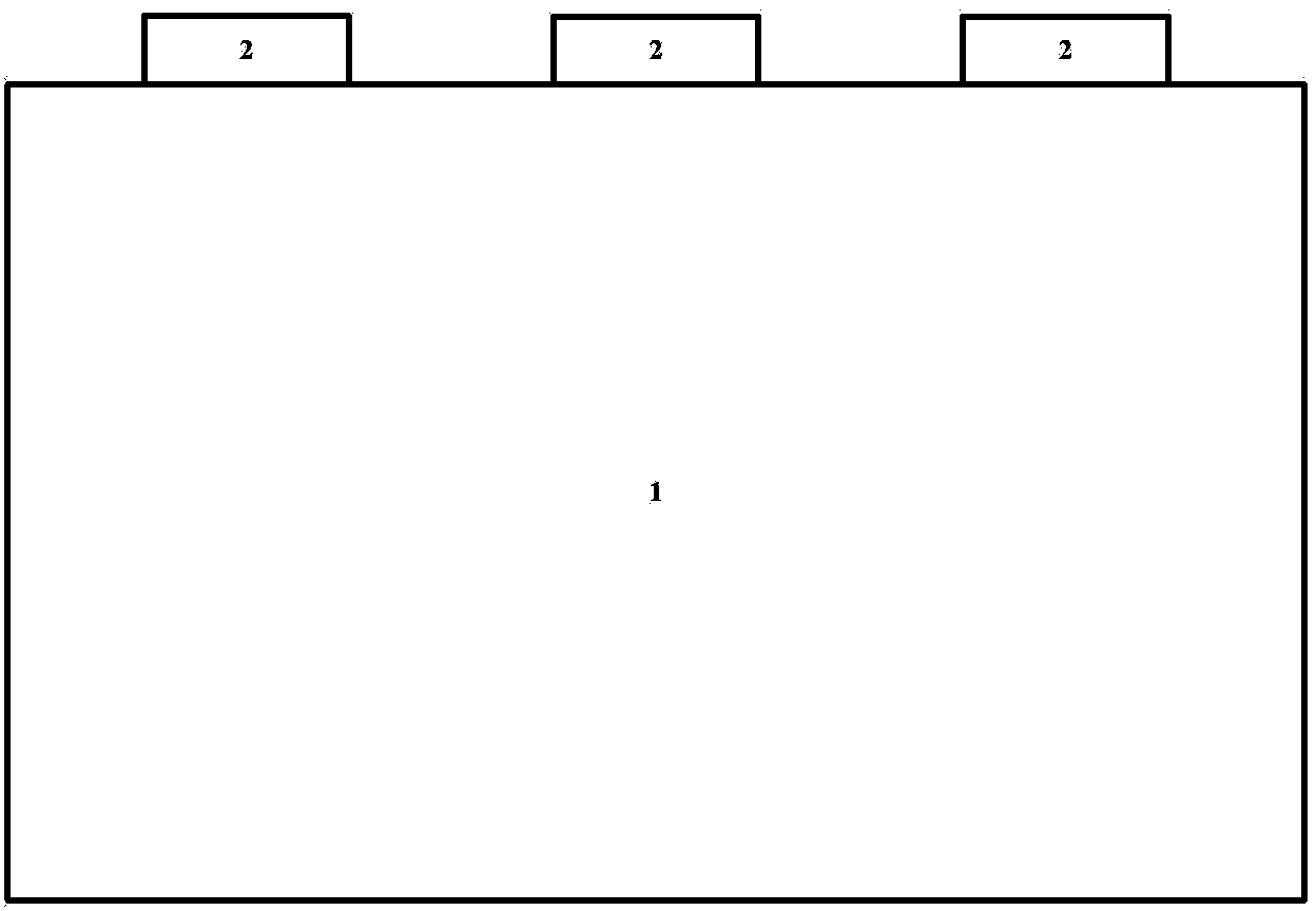
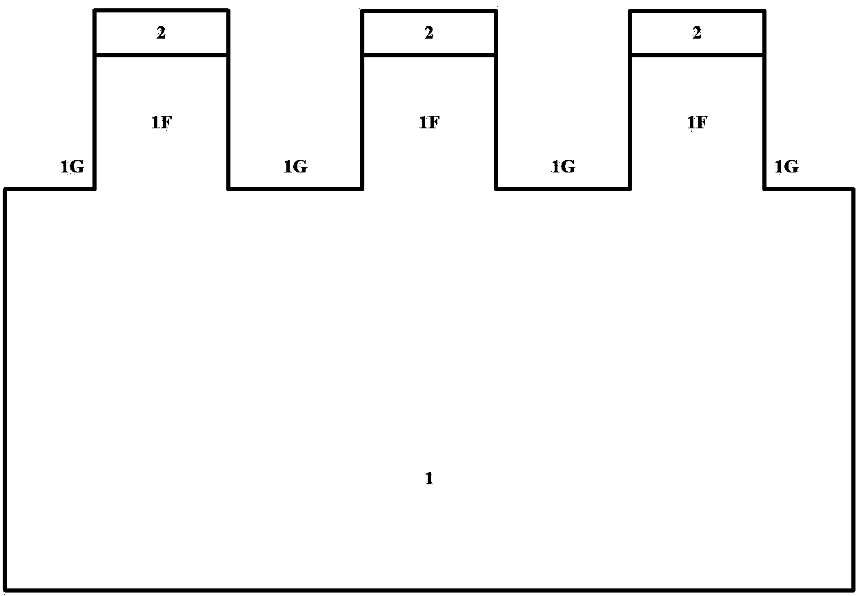
[0029] First, the following will combine Figure 15 flow chart and refer to Figure 1 to Figure 11 A schematic cross-sectional view is used to describe in detail the steps of the semiconductor device manufacturing method according to the first embodiment of the...


PUM


Abstract

The invention discloses a production method of a stacked nanowire. The production method includes steps of a, forming a hard mask on a substrate; b, etching the substrate to form a first trench; c, forming a bottom etching stopping layer at the bottom of the first trench; d, etching the first trench and forming a second trench in the side of the first trench; e, smoothing fins to form the stacked nanowire. According to the arrangement, dry etching is combined with wet etching, vertical pitch is controlled by the dry etching, and the etching stopping layer is injected to control the wet etching, in this way, the precision of the stacked nanowire is increased, and minimization of device is facilitated.

Description

technical field [0001] The invention relates to a method for manufacturing a semiconductor device, in particular to a method for manufacturing stacked nanowires. Background technique [0002] In the current sub-20nm technology, the three-dimensional multi-gate device (FiinFET or Trii-gate) is the main device structure, which enhances the gate control ability and suppresses leakage and short channel effects. [0003] For example, compared with traditional single-gate bulk Si or SOI MOSFETs, MOSFETs with double-gate SOI structures can suppress short-channel effects (SCE) and drain-induced barrier lowering (DIBL) effects, have lower junction capacitance, and can realize The channel is lightly doped, and the threshold voltage can be adjusted by setting the work function of the metal gate, which can obtain about 2 times the driving current and reduce the requirements for the effective gate oxide thickness (EOT). Compared with the double-gate device, the gate of the triple-gate d...

Claims


Application Information

Patent Timeline
IPC IPC(8): H01L21/336H01L21/28B82Y40/00
CPCB82Y10/00B82Y40/00H01L21/30604H01L21/308H01L29/66795
Inventor 马小龙秦长亮殷华湘付作振
Owner INST OF MICROELECTRONICS CHINESE ACAD OF SCI
Why Eureka
Try Eureka