Semiconductor structure and forming method thereof

A semiconductor and morphology technology, applied in semiconductor devices, semiconductor/solid-state device manufacturing, semiconductor/solid-state device components, etc., can solve problems such as chip or device performance degradation, failure, substrate fragmentation, etc., and achieve feature size reduction , The thickness is uniform and dense, and the effect of avoiding substrate fragmentation

Active Publication Date: 2014-12-31
SEMICON MFG INT (SHANGHAI) CORP
View PDF3 Cites 14 Cited by
  • Summary
  • Abstract
  • Description
  • Claims
  • Application Information

AI Technical Summary

Problems solved by technology

[0010] However, when the TSV structure is formed by the existing technology, it is easy to cause the substrate to break, or cause the performance of the chip or device to degrade, or even fail.

Method used


Image

  • Semiconductor structure and forming method thereof
  • Semiconductor structure and forming method thereof
  • Semiconductor structure and forming method thereof

Examples


Embodiment Construction

[0039] As mentioned in the background art, when the TSV structure is formed in the prior art, it is easy to cause the substrate to break, or cause the performance of the chip or device to degrade, or even fail.

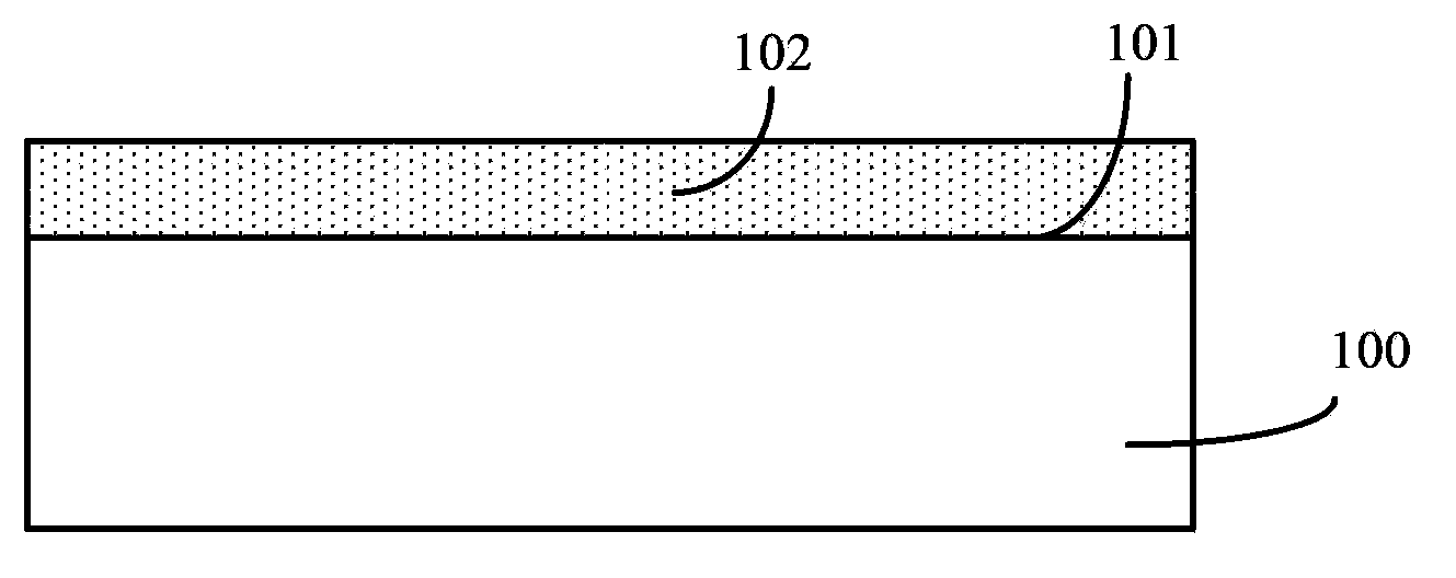
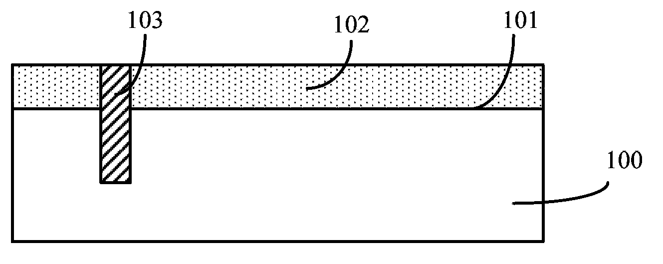
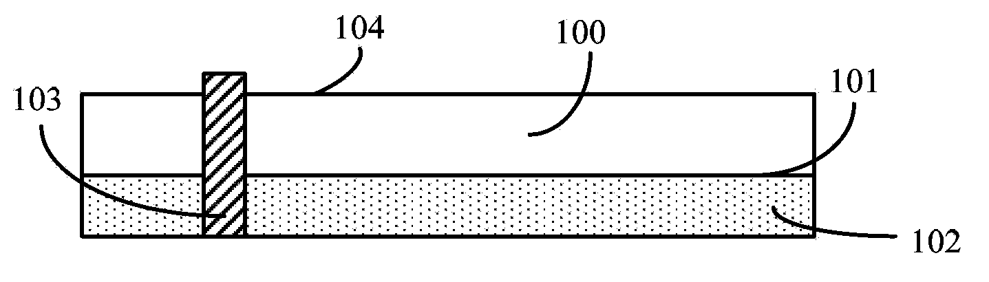
[0040] After research by the inventor of the present invention, please continue to refer to Figure 1 to Figure 3 , the conductive plug 103 is often made of copper; in addition, in order to electrically isolate the conductive plug 103 from the semiconductor substrate 100, an insulating layer is also formed between the conductive plug 103 and the semiconductor substrate 100, The material of the insulating layer is usually silicon dioxide. The thermal expansion coefficient of copper is 18ppm, the thermal expansion coefficient of silicon dioxide is 0.5ppm, and the thermal expansion coefficient of silicon substrate is 2.5ppm. Due to the difference in thermal expansion coefficient between copper, silicon dioxide and silicon substrate, and the thermal expansion coefficient o...


PUM

PropertyMeasurementUnit
thicknessaaaaaaaaaa

Abstract

The invention discloses a semiconductor structure and a forming method thereof. The forming method of the semiconductor structure comprises the steps of providing a substrate which is provided with a plugging area, forming an opening in the substrate, forming a first dielectric layer on the surface of a side wall of the opening by a conformal technology, forming a second dielectric layer at the top of the opening, and forming a conductive plug in the plugging area of the substrate, wherein the opening surrounds the plugging area of the substrate; the pattern of the surface of the first dielectric layer is identical with that of the surface of the side wall of the opening; the second dielectric layer seals the opening; a gap is formed in the opening; and the conductive plug is contacted with the first dielectric layer. The dimension of the semiconductor structure is reduced; the substrate can be prevented from breaking; and reduction of the performance of a chip or a device can be avoided.

Description

technical field [0001] The invention relates to the technical field of semiconductor manufacturing, in particular to a semiconductor structure and a forming method thereof. Background technique [0002] With the continuous development of semiconductor manufacturing technology, the feature size of semiconductor devices is continuously reduced, and the integration level of chips is getting higher and higher. However, the current two-dimensional packaging structure has been difficult to meet the growing demand for chip integration, so three-dimensional packaging technology has become a key technology to overcome the bottleneck of chip integration. [0003] A three-dimensional stacking technology based on through silicon vias (Through Silicon Via, TSV) is one of the existing three-dimensional packaging technologies, and the three-dimensional stacking technology based on through silicon vias is one of the main methods to improve chip integration. [0004] The three-dimensional s...

Claims


Application Information

Patent Timeline
Patent Type & Authority Applications(China)
IPC IPC(8): H01L21/768H01L23/538
CPCH01L23/481H01L21/7682H01L21/76898H01L2924/0002H01L2924/00H01L21/76897H01L21/76835H01L23/5386
Inventor 洪中山
Owner SEMICON MFG INT (SHANGHAI) CORP
Why Eureka
Try Eureka