

Pixel Array Substrate And Panel
A pixel array substrate, pixel technology, applied in the direction of electrical components, electrical solid devices, circuits, etc., can solve the problems of fracture or brittleness of inorganic materials, poor ability, and limit the degree of flexibility of metal wiring areas, and achieve the best structure. The effect of reliability
- Summary
- Abstract
- Description
- Claims
- Application Information
AI Technical Summary
Problems solved by technology
Method used
Image

Examples
Embodiment Construction
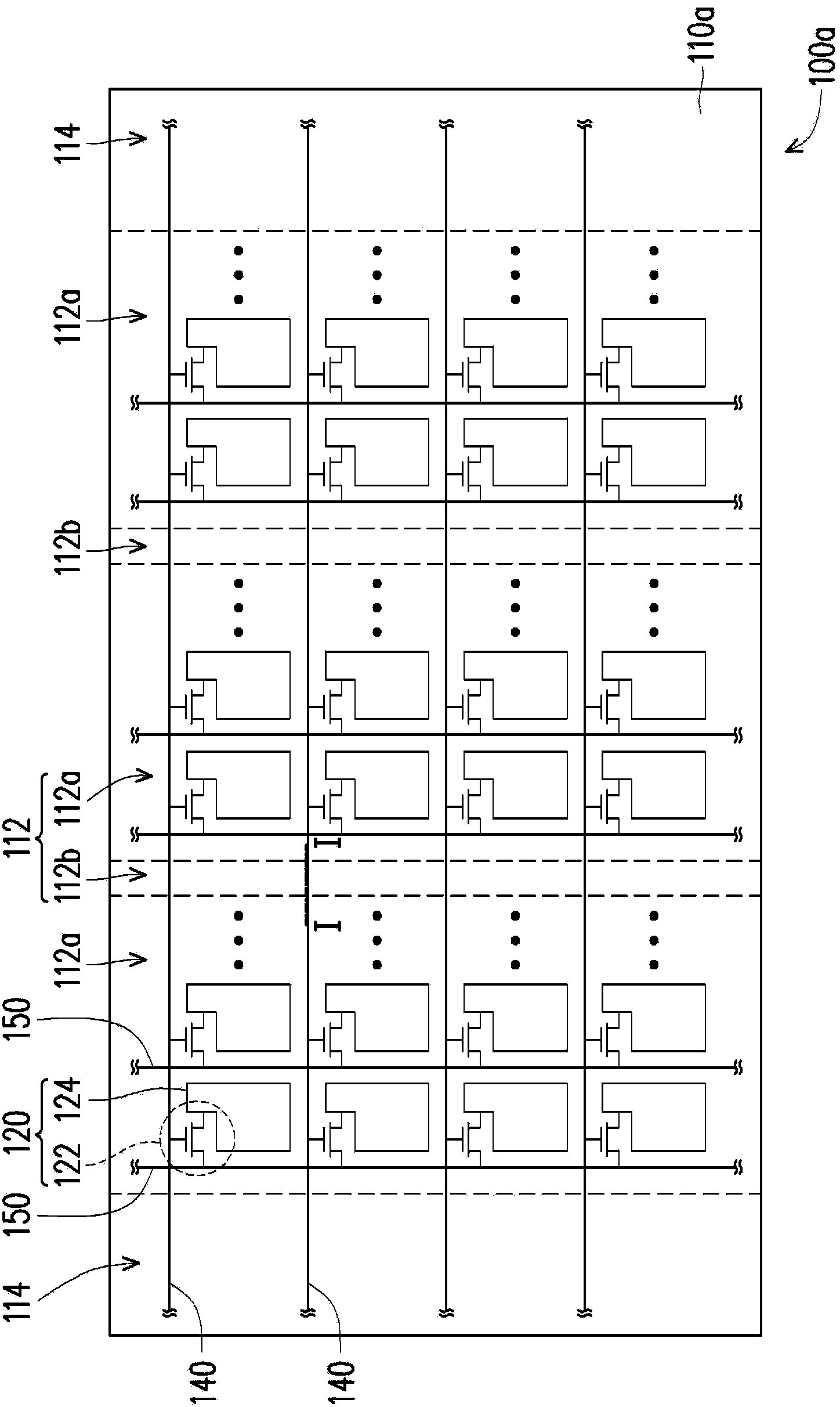
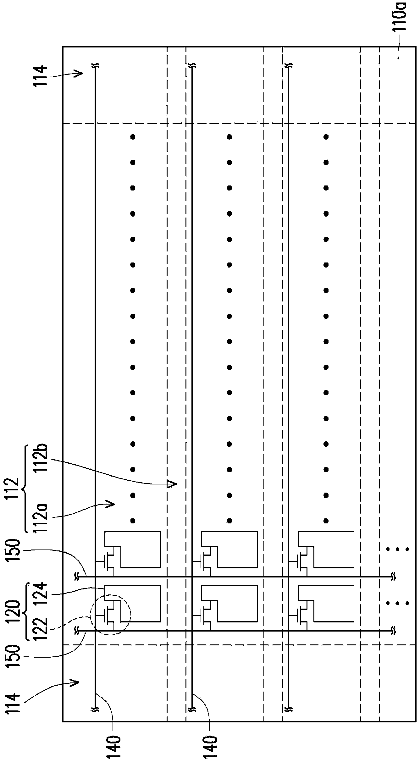
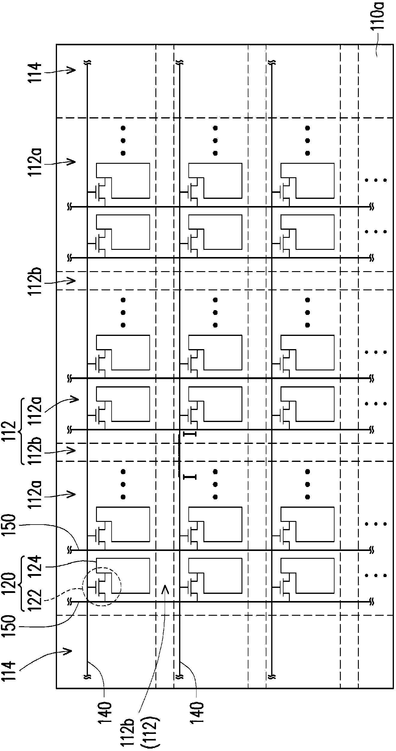
[0059] Figure 1A It is a schematic top view of a pixel array substrate according to an embodiment of the present invention. figure 2 shown along Figure 1A Schematic cross-section of the line I-I. It should be noted that, for the convenience of explanation, Figure 1A Some components are omitted from illustration. Please also refer to Figure 1A and figure 2 , in this embodiment, the pixel array substrate 100 a includes a substrate 110 a, a plurality of pixel units 120 and an inorganic insulating layer 130 . The substrate 110a has an active area 112 and a peripheral area 114 located around the active area 112, wherein the active area 112 includes a plurality of pixel unit areas 112a and a bendable area 112b located on at least one side of the pixel unit area 112a . Each pixel unit 120 includes an active component 122 and a pixel electrode 124 electrically connected to the active component 122 , wherein the pixel electrode 124 is correspondingly disposed in the pixel unit...
PUM
| Property | Measurement | Unit |
|---|---|---|
| Thickness | aaaaa | aaaaa |
| Thickness | aaaaa | aaaaa |
| Thickness | aaaaa | aaaaa |
Abstract
Description
Claims
Application Information