STED (stimulated emission depletion)-based device and method for measuring smooth free-form surface sample

A sample, free technology, applied in measurement devices, optical devices, instruments, etc., can solve problems such as no industrial samples, inability to overcome the extremely weak light intensity of collected signals, etc., to achieve the effect of super-resolution imaging and high-precision measurement

Inactive Publication Date: 2015-01-14
HARBIN INST OF TECH
View PDF6 Cites 14 Cited by
  • Summary
  • Abstract
  • Description
  • Claims
  • Application Information

AI Technical Summary

Problems solved by technology

Since the measurement objects in the field of industrial measurement cannot emit fluorescence, STED microscopy devices are mainly used in the field of biological microscopic imaging, and there is no precedent for application in the shape measurement of industrial samples.
Even if STED microscopy is simply transplanted to the field of industrial sample shape measurement, it cannot overcome the problem that the light intensity of the collected signal is extremely weak due to the specular reflection of the beam on the sample surface with a smooth free-form surface

Method used


Image

  • STED (stimulated emission depletion)-based device and method for measuring smooth free-form surface sample

Examples


Embodiment Construction

[0028] Embodiments of the present invention will be described in detail below in conjunction with the accompanying drawings.

[0029] This embodiment is an embodiment of a device and a method.

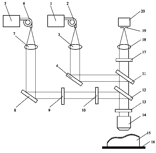
[0030] According to the method of measuring the smooth free-form surface sample device based on STED in this embodiment, the structural diagram is as follows figure 1 shown. The device includes: an excitation module, a loss module, a scanning imaging module and a coating sample 15;

[0031] The excitation module includes: a wavelength of λ 1 The first picosecond pulse laser 1, the first guide fiber 2, the first collimating objective lens 3 and the first plane mirror 4; at a wavelength of λ 1 After the first picosecond pulsed laser 1, the first guide fiber 2, the first collimating objective lens 3 and the first plane mirror 4 are sequentially configured;

[0032] The loss module includes: the wavelength is λ 2 The second picosecond pulse laser 5, the second guide fiber 6, the secon...


PUM


Abstract

The invention relates to an STED (stimulated emission depletion)-based device and method for measuring a smooth free-form surface sample, belonging to the field of the optical microscopic measurement. The device comprises a first picosecond pulse laser, a first conduction optical fiber, a first collimator objective, a first plane reflecting mirror, a second picosecond pulse laser, a second conduction optical fiber, a second collimator objective, a second plane reflecting mirror, a vortex-shaped phase modulation plate, a half-wave plate, a first dichroscope, a second dichroscope, a quarter-wave plate, a focusing object lens, a coating sample, a three-dimensional micro-displacement carrier table, an optical filter, a collection object lens, a pin hole and a photoelectric detector. The surface of the sample is coated with a fluorescent membrane, so that an industrial sample can be measured by utilizing the STED microscopy; meanwhile, the fluorescent membrane radiates fluorescence in different directions under the illumination of the laser, so that the problem that the signal light is difficult to collect caused by the mirror reflection of the light beam on a smooth free-form surface can be avoided. By adopting the device and method, the surface appearance of the smooth sample with a large angle between a normal and the optical axis direction can be high precisely measured.

Description

technical field [0001] The device and method for measuring smooth free-form surface samples based on STED belong to the field of optical microscopic measurement. Background technique [0002] For a sample with a smooth free-form surface, in the area where the angle between the normal line and the optical axis direction is large, the light illuminating the sample surface cannot be completely collected or almost cannot be collected due to specular reflection, so the surface morphology cannot be determined. High-precision measurement, even impossible to measure. Therefore, how to measure a sample with a smooth free-form surface with a large slope with high precision has become a difficult problem in the field of optical measurement. [0003] In the field of sample surface topography measurement, laser scanning confocal microscopy (LSCM) is a commonly used method. This method adopts precise pinhole filtering technology, so that only the information on the focal plane can be de...

Claims


Application Information

Patent Timeline
Patent Type & Authority Applications(China)
IPC IPC(8): G01B11/24
Inventor 刘俭谭久彬张贺刘辰光
Owner HARBIN INST OF TECH
Why Eureka
Try Eureka