Pixel arrangement mode and display panel using same

A pixel and sub-pixel technology, which is applied in the field of pixel layout and display panels using this method, can solve problems such as easy color cast, vapor deposition color mixing, and difficulty in improving image resolution PPI, so as to reduce power consumption and occupancy The area, the effect of improving the physical resolution

Active Publication Date: 2015-01-14
EVERDISPLAY OPTRONICS (SHANGHAI) CO LTD
View PDF7 Cites 17 Cited by
  • Summary
  • Abstract
  • Description
  • Claims
  • Application Information

AI Technical Summary

Problems solved by technology

[0003] However, due to the limitations of the OLED manufacturing process, it is difficult to improve the image resolution PPI (pixel per inch) of the OLED screen, which has become a bottleneck in the development of OLED.
[0004] like figure 1 As shown, the existing display panels generally adopt RGB side by side pixel arrangement, that is, one pixel is formed by three sub-pixels displaying red, green and blue respectively, but this form of arrangement is applied to OLED It is easy to cause vapor deposition mixed color, reduce the pass rate of the product
[0005] According to the characteristics of OLED, a form called Pen Tile pixel arrangement is adopted, and its arrangement form is as follows figure 2 As shown, although this arrangement is conducive to improving the yield of OLED panels, it is not conducive to reflecting the performance of OLED products because its resolution is only 2 / 3 of that of RGB side-by-side arrangement and it is easy to cause color cast.
[0006] "Organic Light Emitting Display Device" (Chinese Patent Publication No. CN102262854A) discloses a pixel arrangement called RGBB, such as image 3 As shown, in view of the fragile characteristics of OLED blue light-emitting devices, the number of sub-pixels emitting blue light is increased in the pixel unit, but it still does not propose a method to increase resolution from the perspective of pixel arrangement

Method used


Image

  • Pixel arrangement mode and display panel using same
  • Pixel arrangement mode and display panel using same
  • Pixel arrangement mode and display panel using same

Examples


Embodiment Construction

[0062] The present invention will be further described below in conjunction with the accompanying drawings and specific embodiments, but not as a limitation of the present invention.

[0063] It should be noted that, in the case of no conflict, the embodiments of the present invention and the features in the embodiments can be combined with each other.

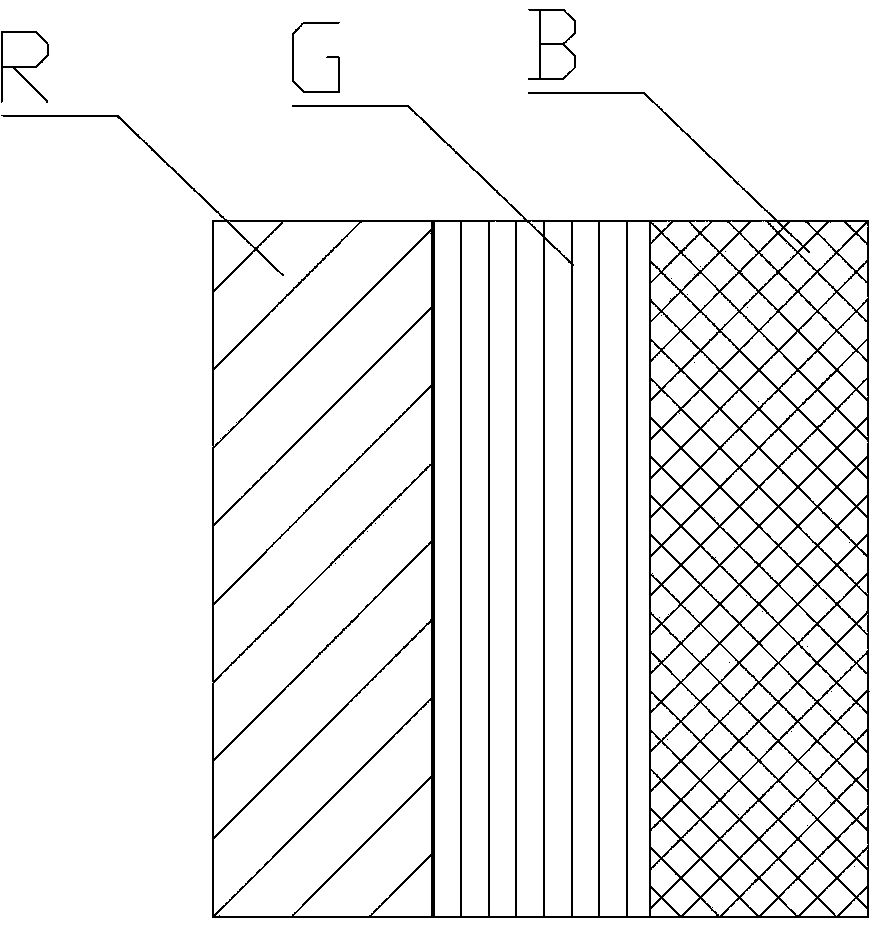
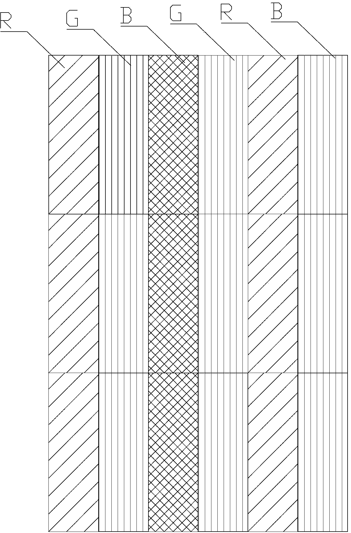
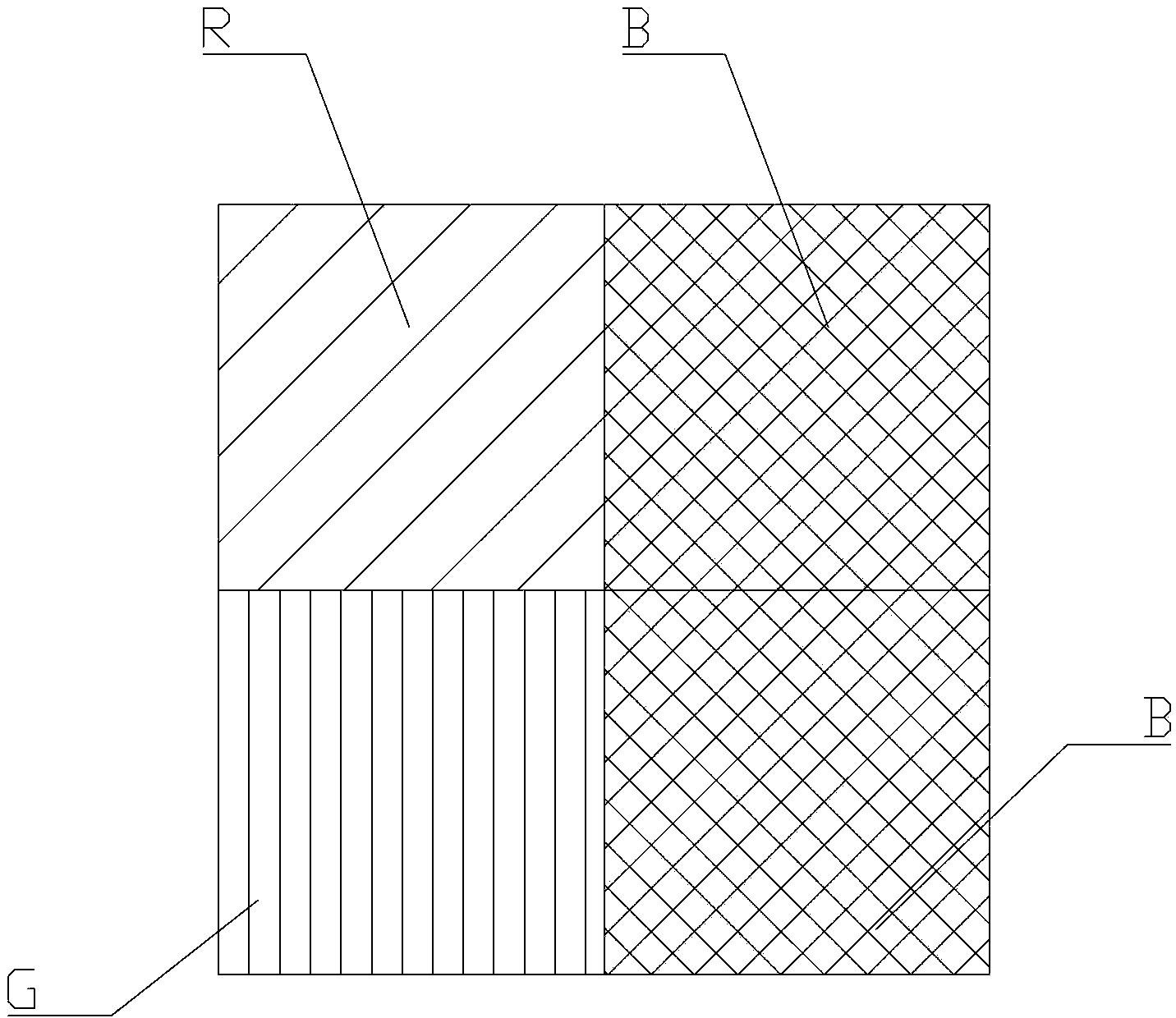
[0064] Such as Figure 4 to Figure 10 As shown, the present invention is a pixel arrangement method, wherein, the display area is divided into a plurality of equal-area rectangular blocks 1 with a vertical grid with equal spacing; The longitudinal axis 12 of the position is divided into a total of four parts: the upper left part 13, the upper right part 14, the lower left part 15 and the lower right part 16; in the four parts of each rectangular block 1, to connect the rectangular area to which each part belongs Each part is divided into two sub-pixel areas by the line connecting the corner of the block and the intersection o...


PUM


Abstract

One embodiment of the present invention discloses a method for pixel arrangement and a display using the same. The display areas are divided into a plurality of rectangular regions which have the same area according to a plurality of vertical grids which own the same distance between the adjacent. According to pre-positioning horizontal axis lines and pre-positioning vertical axis lines, each of the rectangular regions is divided into four parts including an upper left part, an upper right part, a lower left part and a lower right part. Each of the four parts are divided into two sub-pixel areas by a line which is inside the part. The line connects the angle point of the region which the part belongs to and the cross point of the horizontal axis line and the vertical axis line of the region which the part belongs to.

Description

technical field [0001] The present invention relates to a pixel arrangement form, in particular to a pixel arrangement form and a display panel using the form. Background technique [0002] OLED stands for Organic Light-Emitting Diode (Organic Light-Emitting Diode), also known as Organic Electroluminescence Display (OELD). OLED has the characteristic of self-illumination. It uses a very thin organic material coating and glass substrate. When the current passes through, the organic material will emit light, and the OLED display screen has a large viewing angle and can significantly save power. Therefore, the OLED screen has Incomparable advantages of many other flat panel display devices. [0003] However, due to the limitations of the OLED manufacturing process, it is difficult to improve the image resolution PPI (pixel per inch) of the OLED screen, which has become a bottleneck in the development of OLEDs. [0004] Such as figure 1 As shown, the existing display panels g...

Claims


Application Information

Patent Timeline
Patent Type & Authority Applications(China)
IPC IPC(8): G09F9/33
CPCH01L51/56H01L27/3262H01L27/3218H10K59/353H10K59/352
Inventor 黄添旺吴建霖
Owner EVERDISPLAY OPTRONICS (SHANGHAI) CO LTD
Why Eureka
Try Eureka