Metal layer formation process

A metal layer and process technology, applied in the field of metal layer formation technology, can solve problems such as large protrusions of the metal layer, and achieve the effects of reducing contact resistance, uniform grain distribution, and good ohmic contact

Active Publication Date: 2017-05-24
LEADING ENERGY BEIJING ELECTRONICS TECH CO LTD
View PDF5 Cites 0 Cited by
  • Summary
  • Abstract
  • Description
  • Claims
  • Application Information

AI Technical Summary

Problems solved by technology

[0006] The present invention aims to provide a metal layer formation process to solve the problem of large metal layer protrusions in the prior art

Method used


Image

  • Metal layer formation process
  • Metal layer formation process
  • Metal layer formation process

Examples


Embodiment 1

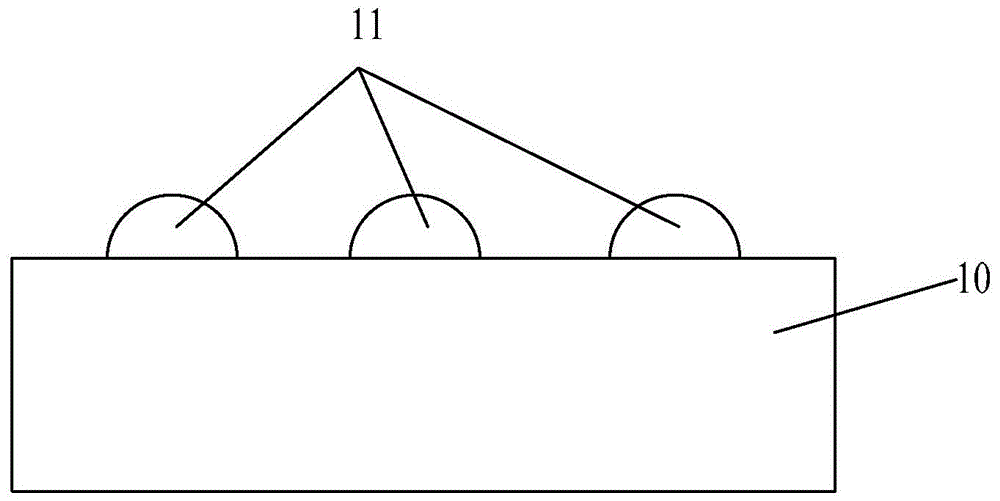
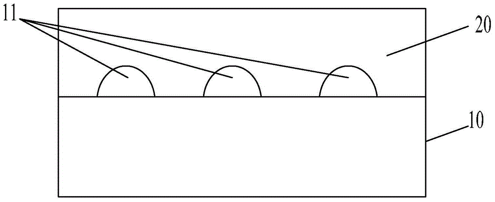
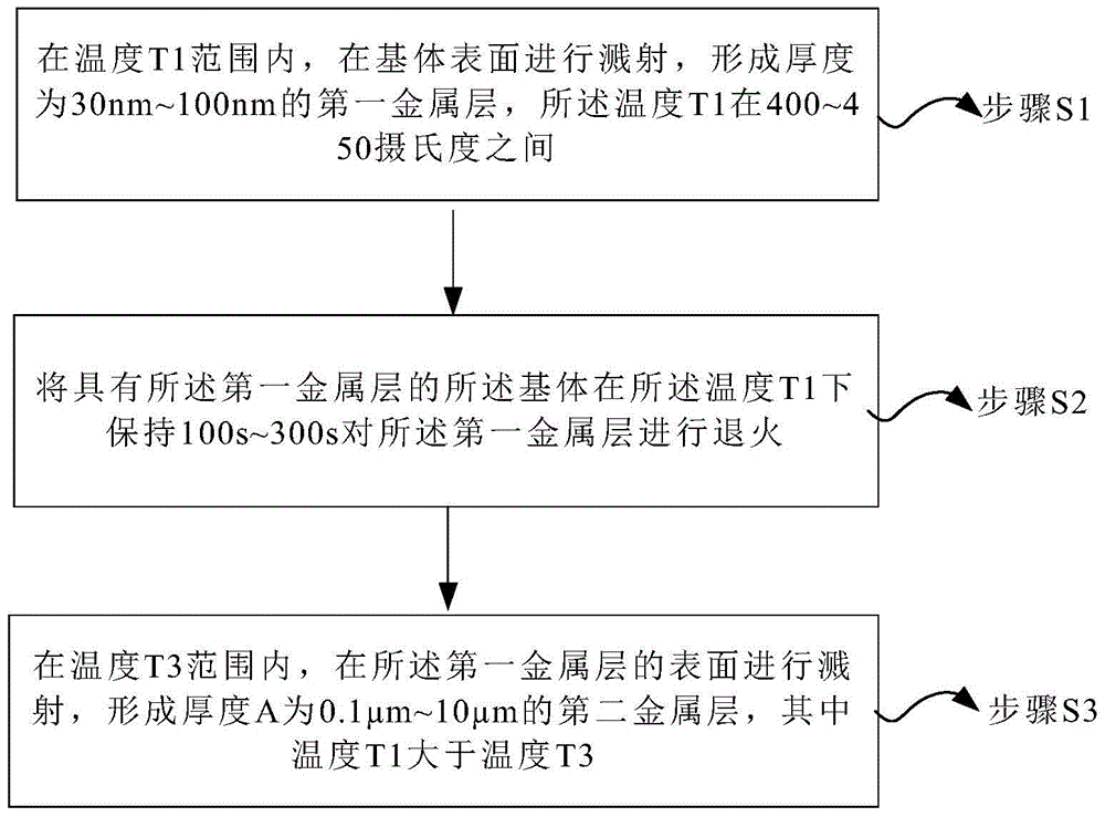
[0049] First, the silicon substrate 30 is transferred from the material box to the vacuum sampling chamber, and after the vacuum chamber is pumped to a high vacuum, the silicon substrate 30 is transferred to the preheating chamber, and the preheating chamber heats the silicon substrate 30 to 450°C, and the time is controlled at Within 300 seconds. The preheating of the silicon substrate 30 makes the temperature of the silicon substrate 30 the same or close to the temperature of the first sputtering, avoiding the sudden temperature rise of the silicon substrate 30 during sputtering to cause its fracture or other physical changes on the surface, ensuring Subsequent sputtering can be performed well.

[0050] The heating temperature of the first sputtering chamber was set at 450° C. to maintain the heating temperature of the silicon substrate 30 . After the silicon substrate 30 is transferred from the preheating chamber to the first sputtering chamber, the sputtering is delayed f...

Embodiment 2

[0059] First, the silicon substrate 30 is transferred from the material box to the vacuum sampling chamber, and after the vacuum chamber is pumped to a high vacuum, the silicon substrate 30 is transferred to the preheating chamber, and the preheating chamber heats the silicon substrate 30 to 450°C, and the time is controlled at Within 300 seconds. The preheating of the silicon substrate 30 makes the temperature of the silicon substrate 30 the same or close to the temperature of the first sputtering, avoiding the sudden temperature rise of the silicon substrate 30 during sputtering to cause its fracture or other physical changes on the surface, ensuring Subsequent sputtering can be performed well.

[0060] The heating temperature of the first sputtering chamber was set at 450° C. to maintain the heating temperature of the silicon substrate 30 . After the silicon substrate 30 is transferred from the preheating chamber to the first sputtering chamber, the sputtering is delayed f...

Embodiment 3

[0063] First, the silicon substrate 30 is transferred from the material box to the vacuum sampling chamber, and after the vacuum chamber is pumped to a high vacuum, the silicon substrate 30 is transferred to the preheating chamber, and the preheating chamber heats the silicon substrate 30 to 450°C, and the time is controlled at Within 300 seconds. The preheating of the silicon substrate 30 makes the temperature of the silicon substrate 30 the same or close to the temperature of the first sputtering, avoiding the sudden temperature rise of the silicon substrate 30 during sputtering to cause its fracture or other physical changes on the surface, ensuring Subsequent sputtering can be performed well.

[0064] The heating temperature of the first sputtering chamber was set at 450° C. to maintain the heating temperature of the silicon substrate 30 . After the silicon substrate 30 is transferred from the preheating chamber to the first sputtering chamber, the sputtering is delayed f...


PUM

PropertyMeasurementUnit
thicknessaaaaaaaaaa
thicknessaaaaaaaaaa
thicknessaaaaaaaaaa

Abstract

The invention provides a forming technology of metal layers. The forming technology comprises the steps that S1, within the range of temperature T1, sputtering is carried out on the surface of a base body, the first metal layer with the thickness of 30 nm to 100 nm is formed, and the temperature T1 ranges from 400 DEG C to 450 DEG C; S2, the base body with the first metal layer is kept for 100 s to 300 s at the temperature T1, and annealing is carried out on the first metal layer; S3, sputtering is carried out on the surface of the first metal layer within the range of temperature T3, the second metal layer with the thickness A of 0.1 micron to 10 microns is formed, and the temperature T1 is larger than the temperature T3. The forming technology of the metal layers solves the problem that protrusions are formed on the surface of metal through a traditional sputtering method, a smooth metal surface can be formed, and then the good device performance is guaranteed.

Description

technical field [0001] The invention relates to the field of semiconductors, in particular to a process for forming a metal layer. Background technique [0002] Generally, a typical process for forming an Al-Si ohmic contact for a standard silicon device generally includes: step S1', forming the metal aluminum layer 10 by sputtering aluminum-silicon-copper (AlSiCu) process, and step S2', annealing the metal aluminum layer to make it Form a good ohmic contact with the silicon substrate. [0003] In the above-mentioned typical process, many hillock-shaped protrusions 11 of different degrees will appear on the surface of the metal aluminum layer 10 . Such as figure 1 As shown, the reason for the formation of protrusions 11: on the one hand, the crystal grains formed by the sputtering of metal aluminum during the sputtering process of step S1' cannot be absolutely uniform, so they will be formed on the surface of the metal aluminum layer 10 formed by sputtering A small amount...

Claims


Application Information

Patent Timeline
Patent Type & Authority Patents(China)
IPC IPC(8): H01L21/02H01L21/28
CPCH01L21/02697H01L21/283
Inventor 义夫
Owner LEADING ENERGY BEIJING ELECTRONICS TECH CO LTD
Why Eureka
Try Eureka