Hybrid waveguide laser and method for manufacturing hybrid waveguide laser

一种波导激光器、波导的技术,应用在半导体激光器、激光器、激光器零部件等方向,能够解决高制造成本等问题,达到低阈值、小器件尺寸、改善散热的效果

Active Publication Date: 2015-01-14
INTERUNIVERSITAIR MICRO ELECTRONICS CENT (IMEC VZW) +1
View PDF3 Cites 11 Cited by
  • Summary
  • Abstract
  • Description
  • Claims
  • Application Information

AI Technical Summary

Problems solved by technology

However, this approach leads to relatively high fabrication costs due to the extreme consumption of expensive III-V materials

Method used


Image

  • Hybrid waveguide laser and method for manufacturing hybrid waveguide laser
  • Hybrid waveguide laser and method for manufacturing hybrid waveguide laser
  • Hybrid waveguide laser and method for manufacturing hybrid waveguide laser

Examples


Embodiment Construction

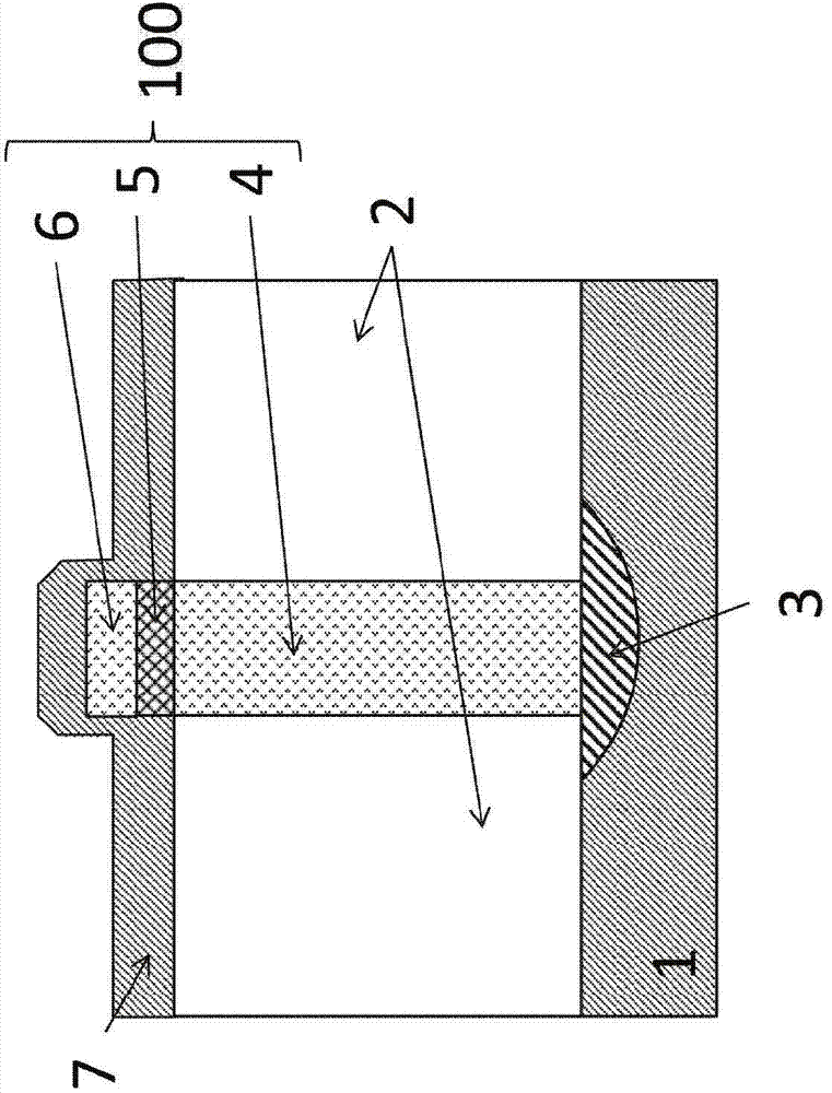
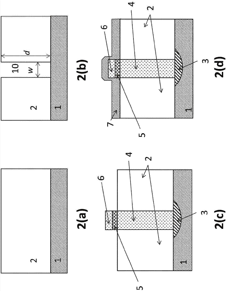
[0033] In the following detailed description, numerous specific details are set forth in order to provide a thorough understanding of the disclosure and how it may be practiced in certain embodiments. However, it is understood that the present disclosure may be practiced without these specific details. In other instances, well-known methods, procedures and techniques have not been described in detail so as not to obscure the present disclosure. Although the present disclosure will be described with respect to particular embodiments and with reference to certain drawings, the present disclosure is not limited thereto. The drawings included and described herein are schematic and do not limit the scope of the present disclosure. It should also be noted that in the drawings, the size of some of the elements may be exaggerated for illustrative purposes and therefore not drawn on scale.

[0034] The present invention will be described with respect to particular embodiments and wit...


PUM


Abstract

The invention relates to a hybrid waveguide laser and a method for manufacturing the hybrid waveguide laser. The hybrid waveguide laser is sub-micron III-V in level and comprises a channel waveguide, a lateral cladding layer adjacent to the waveguide in the transverse direction, and a light limiting element. The channel waveguide is 50 nm to 800 nm in width and 500 nm to 1200 nm in height. The light limiting element is used for limiting the light within the waveguide. The waveguide may comprise an III-V lamination comprising a lower cladding layer, an active region and an upper cladding layer. The laser may be optically coupled to an output waveguide which may be electrically pumped. The invention also provides a method for integrating the sub-micron III-V level waveguide laser onto a silicon photon platform. The method comprises the steps of providing an electricity insulating layer on a silicon substrate, etching a channel of 50 nm to 800 nm in width in the electricity insulating layer, forming a channel waveguide in the channel through providing an III-V lamination during the local epitaxial growth process, and providing a light limiting element to limit the light within the waveguide.

Description

technical field [0001] The disclosed technology relates to hybrid waveguide lasers (eg, submicron hybrid waveguide lasers) and methods for integrating such waveguide lasers on silicon photonics platforms. Background technique [0002] Driven by demands from optical I / O, telecommunications, optical computing, and other applications, much research is being done in the area of ​​integrating III-V devices on silicon. Various options have been proposed for integrating electrically pumped lasers and optical amplifiers on silicon-based photonics platforms. [0003] The individual laser dies can be flip-chip mounted to a silicon photonics wafer or can be transferred to a silicon platform using an epitaxial lift-off process. Tight mechanical alignment requirements make this option less attractive, especially for wavelength-division multiplexing (WDM) systems where the number of lasers required per chip has increased over the past few years. [0004] Alternatively, bonding methods c...

Claims


Application Information

Patent Timeline
Patent Type & Authority Applications(China)
IPC IPC(8): H01S3/063H01S5/02315
CPCH01S5/021H01S5/026H01S5/2027H01S5/2214H01S5/2218H01S5/2272H01S2301/176G02B6/12004G02B6/1228G02B2006/12078G02B2006/12121H01S5/02315H01S5/0233H01S5/2077H01S5/042H01S5/3013H01S5/0203H01S5/0235
Inventor D·范托尔豪特Z·王J·范卡姆潘豪特M·潘图瓦基
Owner INTERUNIVERSITAIR MICRO ELECTRONICS CENT (IMEC VZW)
Why Eureka
Try Eureka