Chip test board and chip test system

A technology for testing chips and chips to be tested, which is applied in the direction of electronic circuit testing, measuring electronics, and measuring devices. area effect

Active Publication Date: 2015-01-28
SINO IC TECH
View PDF6 Cites 6 Cited by
  • Summary
  • Abstract
  • Description
  • Claims
  • Application Information

AI Technical Summary

Problems solved by technology

[0007] The purpose of the present invention is to provide a chip test board and a chip test system, to solve the problem of high manufacturing cost of the chip test board and inaccurate test results, using various types of chip test

Method used


Image

  • Chip test board and chip test system
  • Chip test board and chip test system
  • Chip test board and chip test system

Examples


Embodiment 1

[0032] The invention provides a chip testing system, comprising: a signal generating unit, a processing unit, a display unit, a chip testing board and a chip to be tested located on the chip testing board, wherein,

[0033] The signal generating unit generates an excitation signal for the chip to run;

[0034] The processing unit is used to monitor or analyze the operating state of the chip, and transmit the monitored state or the analysis result to the display unit;

[0035] The display unit is used to display the status or result of chip operation.

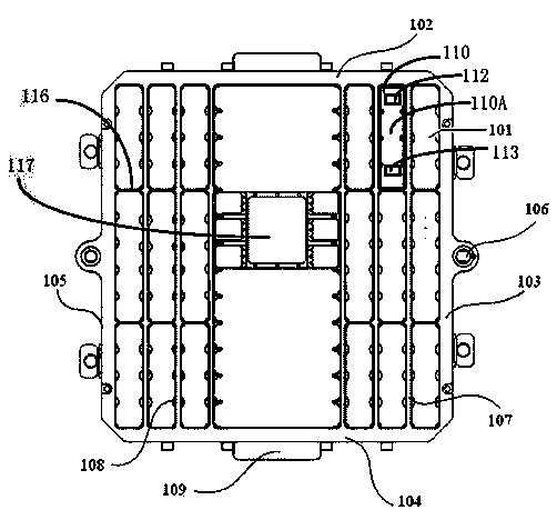
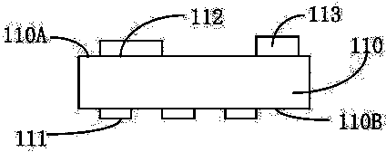
[0036] Specifically, such as figure 1 and image 3 As shown, the chip test board includes: a fixed frame 101 formed by vertically connecting successively the first crossbar, the second crossbar, the third crossbar, and the fourth crossbar (102, 103, 104, 105), and At least one PCB board 110 detachably connected to the fixing frame 101 allows the PCB board 110 to be selectively placed in the fixing frame 101 . According to th...

Embodiment 2

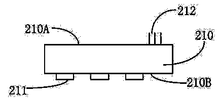
[0046] Such as figure 1 and Figure 4 As shown, the back side 210B of the PCB board 210 is provided with a pogo pin copper clad plate 211 electrically connected to the test machine, and the front side 210A of the PCB board 210 is provided with an electrical channel that can lead out the test machine to connect with the chip test board. The leading end 212 of the signal. The lead end 212 is connected to the chip under test. At the same time, the lead-out end can also be connected to the test base 113 on another PCB board 110 on the same fixed frame 101, and a plurality of PCB boards (110, 210) of different sizes can be formulated for combined use according to actual needs, reducing The size of a single PCB board is small, and PCB boards of different sizes can be reused to reduce costs.

[0047] Other parts are the same as those in Embodiment 1, and will not be repeated here.

[0048] To sum up, in the chip test board and the chip test system provided by the embodiments of t...


PUM


Abstract

The invention provides a chip test board and a chip test system. The chip test board comprises a fixing frame formed by sequentially and vertically connecting a first cross rod, a second cross rod, a third cross rod and a fourth cross rod, and at least one PCB detachably connected with the fixing frame, wherein the PCB can be selectively arranged in the fixing frame. At least one PCB is detachably connected to the fixing frame, corresponding sizes of PCBs are designed according to the test demands of different devices, different quantities of PCBs can be further selected according to the actual demand, a plurality of PCBs are combined in use to share test resources and achieve resource reuse, the manufacturing area of the single PCB is decreased, cost is reduced, and the PCB is selectively arranged in the fixing frame, so that resources on a testing machine are reasonably utilized. The PCB and the fixing frame are simple to mount and dismount and convenient to operate.

Description

technical field [0001] The invention relates to the technical field of integrated circuit manufacturing equipment, in particular to a chip test board and a chip test system applied to an integrated circuit automatic test system. Background technique [0002] At present, integrated circuits are gradually being applied to many fields, such as computers, communications, industrial control and consumer electronics. The manufacturing of integrated circuits has become the same basic industry as steel. [0003] After the wafer has undergone complicated manufacturing processes such as exposure, etching, ion implantation, deposition, and growth, and after the chip is formed and packaged, various extremely strict tests are required, such as electrical parameter testing on the automatic test system (ATE), Functional tests, etc., can only be delivered to customers until they pass the test. [0004] The existing chip test board mainly has the following two methods: [0005] The first ...

Claims


Application Information

Patent Timeline
Patent Type & Authority Applications(China)
IPC IPC(8): G01R1/02G01R31/28
Inventor 王华刘远华王锦季海英邓维维郝丹丹
Owner SINO IC TECH
Why Eureka
Try Eureka