Wavefront measuring chip based on electrically-controlled liquid crystal converging micro lens

A technology of wavefront measurement and microlens, applied in measuring devices, measuring optics, optical radiation measurement, etc., can solve the problems of insufficient efficiency and high cost, and achieve the effects of good adaptability, high measurement accuracy, and high control accuracy

Active Publication Date: 2015-02-04
HUAZHONG UNIV OF SCI & TECH
View PDF4 Cites 16 Cited by
  • Summary
  • Abstract
  • Description
  • Claims
  • Application Information

AI Technical Summary

Problems solved by technology

In view of the above situation, at present, it is mainly through the transformation of the main optical system, the development of special image information processing algorithms, and the construction of placing the microlens array on the MEMS structure to adjust the distance between the CCD or CMOS photosensitive array. Limited effect, high cost, serious lack of performance, urgent need for new technical support means

Method used


Image

  • Wavefront measuring chip based on electrically-controlled liquid crystal converging micro lens
  • Wavefront measuring chip based on electrically-controlled liquid crystal converging micro lens
  • Wavefront measuring chip based on electrically-controlled liquid crystal converging micro lens

Examples


Embodiment Construction

[0023]In order to make the object, technical solution and advantages of the present invention clearer, the present invention will be further described in detail below in conjunction with the accompanying drawings and embodiments. It should be understood that the specific embodiments described here are only used to explain the present invention, not to limit the present invention. In addition, the technical features involved in the various embodiments of the present invention described below can be combined with each other as long as they do not constitute a conflict with each other.

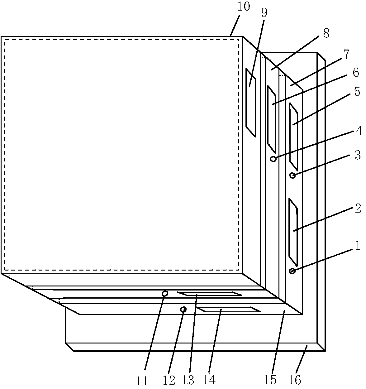
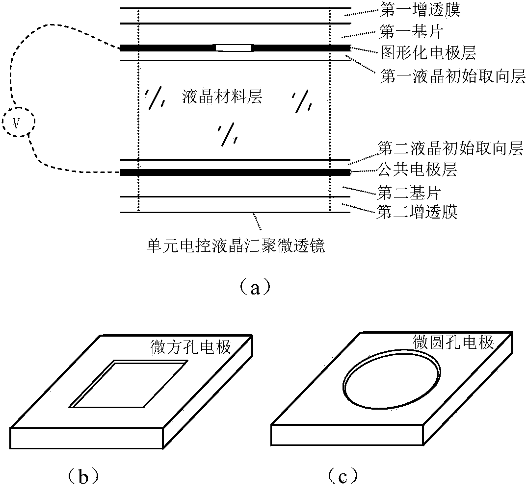
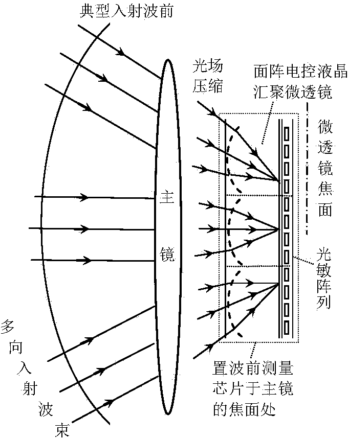
[0024] Such as figure 1 As shown, the wavefront measurement chip based on the electronically controlled liquid crystal converging microlens in the embodiment of the present invention includes a chip housing 15 , a wavefront measurement structure and a metal support cooling plate 16 . The wavefront measurement architecture includes a drive control preprocessing module 7 , an area array visible li...


PUM

PropertyMeasurementUnit
porosityaaaaaaaaaa

Abstract

The invention discloses a wavefront measuring chip based on an electrically-controlled liquid crystal converging micro lens. The wavefront measuring chip comprises an area array electrically-controlled liquid crystal converging micro lens and an area array visual light detector; the area array electrically-controlled liquid crystal converging micro lens comprises a liquid crystal material layer, a first liquid crystal initial orientating layer, a graphical electrode layer, a first substrate, a first antireflection film, a second liquid crystal initial orientating layer, a common electrode layer, a second substrate and a second antireflection film, wherein the first liquid crystal initial orientating layer, the graphical electrode layer, the first substrate and the first antireflection film are sequentially arranged on the upper surface of the liquid crystal material layer; the second liquid crystal initial orientating layer, the common electrode layer, the second substrate and the second antireflection film are sequentially arranged on the lower surface of the liquid crystal material layer; the common electrode layer is composed of a homogenous conductive film layer; the graphical electrode layers are composed of a humongous conductive film layer on which square holes or circular holes are distributed like an m*n array; the area array visual light detector is divided into secondary area array visual light detectors which are distributed like the m*n array; each secondary area array visual light detector includes light-sensitive elements which are distributed like a j*j array. According to the chip, the wavefront measuring range is large, the adaptability of target and environment is high, and an optical and photoelectric mechanical structure is easily coupled.

Description

technical field [0001] The invention belongs to the technical field of optical precision measurement and control, and more specifically relates to a wavefront measurement chip based on an electrically controlled liquid crystal converging microlens. Background technique [0002] Wavefront is a basic parameter that characterizes light waves. Timely and accurate acquisition of the wavefront information of the transmission light field is to analyze the spatiotemporal evolution behavior of light waves, the interaction properties with the material structure, the influence of the environmental medium on the transmission light field, the ability to carry and transmit the target image information and its change characteristics, As well as the basis and premise of controlled modulation of the light field. To date, a wide variety of wavefront direct and indirect measurement methods have been developed. In the wavefront measurement means with small and miniaturized features, the fast ...

Claims


Application Information

Patent Timeline
Patent Type & Authority Applications(China)
IPC IPC(8): G01J9/00G02F1/29G02F1/133
Inventor 张新宇佟庆雷宇罗俊桑红石谢长生
Owner HUAZHONG UNIV OF SCI & TECH
Why Eureka
Try Eureka