Infrared liquid crystal phased array chip

A liquid crystal phase and liquid crystal technology, applied in the field of infrared liquid crystal phased array chips, can solve the problems of narrow spectrum application range, single function, slow response, etc., and achieve the effects of flexible control mode, high control precision and convenient connection

Active Publication Date: 2015-02-04
HUAZHONG UNIV OF SCI & TECH
View PDF5 Cites 12 Cited by
  • Summary
  • Abstract
  • Description
  • Claims
  • Application Information

AI Technical Summary

Problems solved by technology

The main technical defects are manifested in the following aspects: (1) The volume, mass and inertia of the optical and auxiliary actuators are large, the function is relatively single, and a relatively complicated drive and control device needs to be configured, the response is slow, and the state transition time is long. Continuity makes it difficult to construct, switch or jump the beam state arbitrarily; (2) The infrared optical components used such as typical prisms, lenses, reflectors and astigmatism mirrors, as well as the various optical films produced such as typical Reflective, anti-reflective and semi-reflective and semi-transparent films, etc., all have a relatively narrow spectral range of application, and there are chromatic aberrations or aberrations that are difficult to completely offset with changes in infrared spectral components
Beam space scanning is often realized based on the reciprocating mechanical translation between the pendulum mirror or the microlens array. There is a single scanning mode constrained by special rotation or translation, limited performance indicators, large mechanical inertia, and relatively complex auxiliary drives. control device, the state change is slow, the beam scanning operation can only be carried out in accordance with the set order, and any form of beam scanning cannot be realized, regional cohesion and scanning are difficult to coexist or fast switching and other defects

Method used


Image

  • Infrared liquid crystal phased array chip
  • Infrared liquid crystal phased array chip
  • Infrared liquid crystal phased array chip

Examples


Embodiment Construction

[0020] In order to make the object, technical solution and advantages of the present invention clearer, the present invention will be further described in detail below in conjunction with the accompanying drawings and embodiments. It should be understood that the specific embodiments described here are only used to explain the present invention, not to limit the present invention. In addition, the technical features involved in the various embodiments of the present invention described below can be combined with each other as long as they do not constitute a conflict with each other.

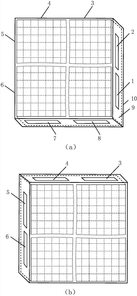
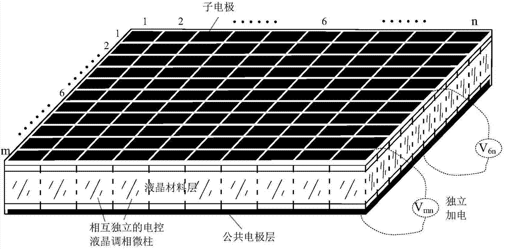
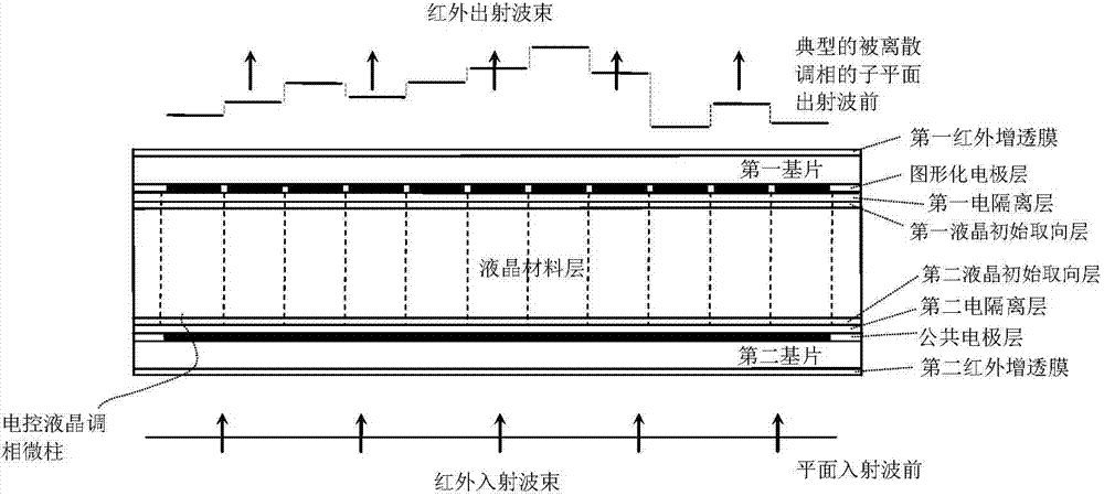
[0021] like figure 1 As shown, the infrared liquid crystal phased array chip of the embodiment of the present invention includes a chip housing 10 and an electronically controlled liquid crystal phase modulation microcolumn array 9 . The electronically controlled liquid crystal phase modulation microcolumn array 9 is packaged in the chip case 10 and is fixedly connected with the chip case 10 , ...


PUM


Abstract

The invention discloses an infrared liquid crystal phased array chip. The chip comprises an electric control liquid crystal phase modulation microcolumn array; the electric control liquid crystal phase modulation microcolumn array comprises a liquid crystal material layer, a liquid crystal initial orientation layer, an electric isolation layer, a patterned electrode layer, a substrate and an infrared antireflection film which are sequentially arranged on the upper surface of the liquid crystal material layer, and a liquid crystal initial orientation layer, an electric isolation layer, a public electrode layer, a substrate and an infrared antireflection film which are sequentially arranged on the lower surface of the liquid crystal material layer; the patterned electrode layer is composed of sub-electrodes which are distributed in an arrayed manner, and each sub-electrode is composed of square or rectangular conductive films; the electric control liquid crystal phase modulation microcolumn array is divided into electrode control liquid crystal phase modulation microcolumns which are distributed in an arrayed manner, the electrode control liquid crystal phase modulation microcolumns correspond to the sub-electrodes one by one, and the rate of the area of each sub-electrode to the optical receiving area of the corresponding electrode control phase crystal phase modulation microcolumn is 50-95 percent. The chip can realize the functions of electric control beam expanding, beam contracting, debunching, beam concentrating, beam tuning, beam scanning and the like, is easy to couple with other infrared optical and photoelectric mechanical structures and has good optical field adaptability.

Description

technical field [0001] The invention belongs to the technical field of infrared beam precision measurement and control, and more specifically relates to an infrared liquid crystal phased array chip. Background technique [0002] So far, based on the electromagnetic wave phase modulation technology, the radio frequency phased array technology that realizes the arbitrary shape construction of the electromagnetic beam, adjustable direction projection, electronically controlled space scanning, specific orientation or airspace beam condensation, etc., has shown strong performance in the radar field. It has become a research and development hotspot in infrared beam engineering to find a method for electromagnetic beam phase modulation suitable for infrared bands, and to realize beam building, beam projection, and beam space scanning functions similar to radio frequency electromagnetic waves. With the continuous and rapid development of infrared beam technology and the continuous e...

Claims


Application Information

Patent Timeline
IPC IPC(8): G02F1/1343G02F1/133G02F1/29G01J3/12
CPCG01J3/12G02F1/1313G02F1/1333G02F1/1335G02F1/1343
Inventor 张新宇罗俊佟庆雷宇桑红石谢长生
Owner HUAZHONG UNIV OF SCI & TECH
Why Eureka
Try Eureka