
Mask level reduction for mofet

A technology of mask and oxide layer, applied in the field of mask level reduction for MOFET

Inactive Publication Date: 2015-02-04
CBRITE
View PDF5 Cites 6 Cited by
  • Summary
  • Abstract
  • Description
  • Claims
  • Application Information

AI Technical Summary

Problems solved by technology

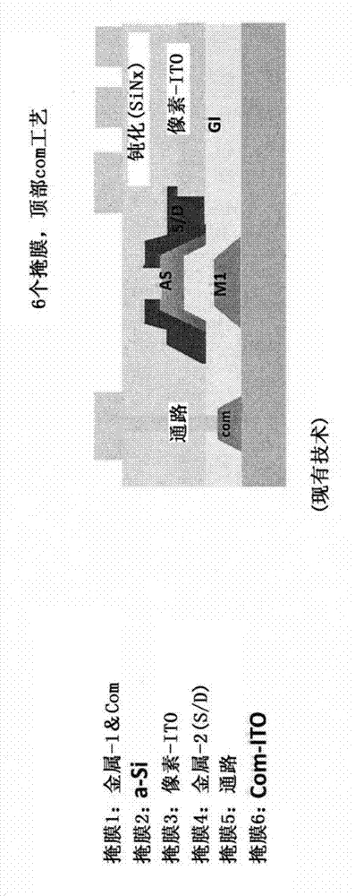
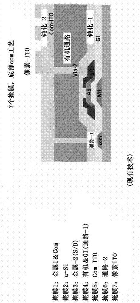
The problem with IPS type LCDs is that two patterned transparent electrodes are required which results in the need for seven (7) patterning steps

Method used


Image

  • Mask level reduction for mofet
  • Mask level reduction for mofet
  • Mask level reduction for mofet

Examples


Embodiment Construction

[0014] specific reference figure 1 , illustrating a simplified cross-sectional view of a state-of-the-art in-plane switching (IPS) in an active-matrix liquid crystal display (AMLCD). Although only a single element is illustrated for convenience throughout the specification, it should be understood that a complete display consists of a matrix of pixels each including one or more of the individual elements shown. This single component includes the LCD and field effect transistor (FET) pixel drivers, which are typically thin film transistors (TFT). The TFT is activated or controlled by a scan line connected to a gate and a data line connected to a source / drain (S / D) terminal.

[0015] exist figure 1 In the state of the art or state-of-the-art for in-plane switching (IPS) and TFTs, a substrate (glass) is provided and the gate (M1) and electrical connections (COM) are patterned on this substrate in a first patterning step . A gate dielectric insulator (GI) and an active layer o...


PUM


Abstract

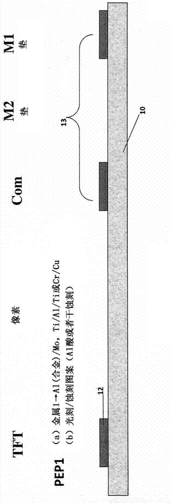
A method of fabricating a TFT and IPS with reduced masking operations includes a substrate, a gate, a layer of gate dielectric on the gate and surrounding substrate surface and a semiconducting metal oxide on the gate dielectric. A channel protection layer overlies the gate to define a channel area in the semiconducting metal oxide. A S / D metal layer is patterned on the channel protection layer and a portion of the exposed semiconducting metal oxide to define an IPS area. An organic dielectric material is patterned on the S / D terminals and at an opposed side of the IPS area. The S / D metal is etched to expose the semiconducting metal oxide defining a first IPS electrode. A passivation layer covers the first electrode and a layer of transparent conductive material is patterned on the passivation layer to define a second IPS electrode overlying the first electrode.

Description

technical field [0001] The present invention generally relates to processes in which the number of masks is reduced in active matrix production. Background technique [0002] In active matrix liquid crystal displays (AMLCDs) and active matrix organic light emitting displays (AMOLEDs), conductive layers for different functions are required. For example, a metal layer is required for scan lines and another metal layer is required for data lines. These two lines cross each other and cannot be formed during the same metal level step. The conductivity of metal lines for data lines and scan lines is very critical and cannot be made of relatively low conductivity transparent materials due to the required conductivity. Also, a transparent conductive layer is required as an electrode for a transmission type LCD or a bottom emission type OLED. Combining with other metal lines or forming transparent conductors is not easy. Each metal line needs to be patterned in a different photol...

Claims


Application Information

Patent Timeline
IPC IPC(8): G02F1/1343
CPCG02F1/134363G02F1/136227G02F1/13439G02F1/1368G02F1/134372G02F1/136231G02F1/136236H01L27/1225H01L27/1288
Inventor 谢泉隆俞钢法特·弗恩格李刘中
Owner CBRITE
Learn More