
Forming method of semiconductor device
A semiconductor and device technology, applied in the field of semiconductor device formation, can solve problems such as large threshold voltage mismatch
- Summary
- Abstract
- Description
- Claims
- Application Information
AI Technical Summary
Problems solved by technology
Method used
Image

Examples
Embodiment 1
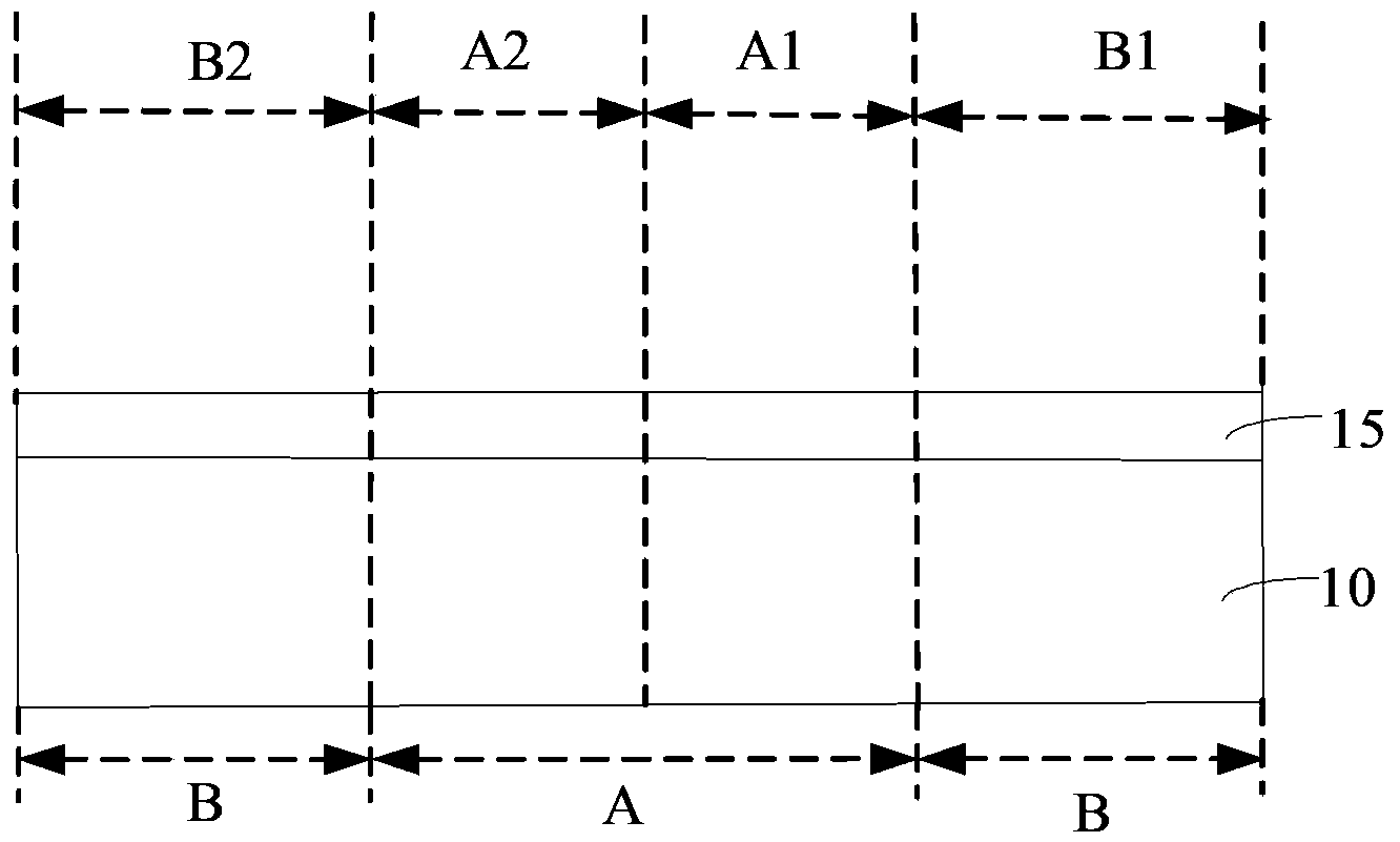
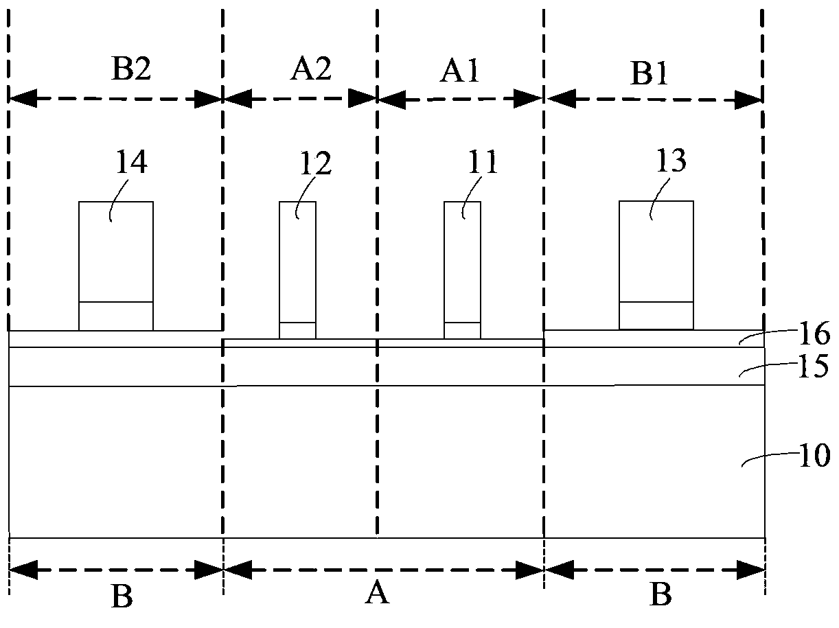
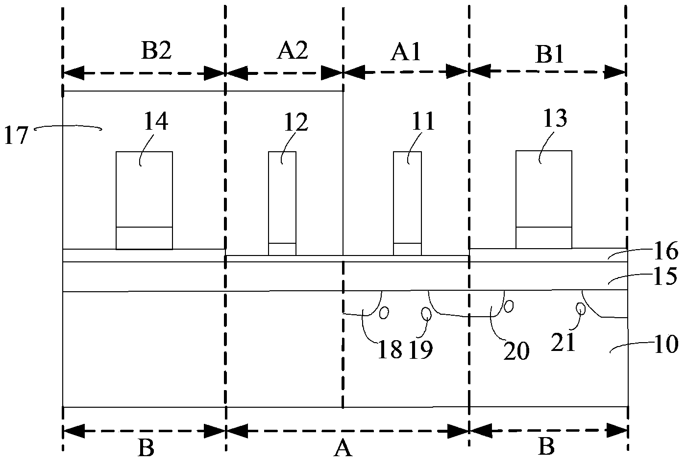
[0061] refer to Figure 6 , providing a substrate 30, the substrate 30 includes a core device area A and a peripheral circuit area B; the core device area A includes: a first PMOS area A1 and a first NMOS area A2, and the peripheral circuit area B includes: The second PMOS area B1 and the second NMOS area B2.
[0062] Specifically, the semiconductor substrate 30 may be at least one of the materials mentioned below: silicon, silicon-on-insulator (SOI), silicon-on-insulator (SSOI), silicon-germanium-on-insulator (S-SiGeOI) and Silicon germanium on insulator (SiGeOI), etc. A doped region and an isolation structure may be formed in the substrate, and the isolation structure is a shallow trench isolation (STI) structure or a local oxide of silicon (LOCOS) isolation structure.
[0063] refer to Figure 7 , performing threshold voltage implantation on the surface of the substrate 30 to form a threshold voltage injection layer 35 .
[0064]The threshold voltage injection layer 35 ...
Embodiment 2
[0125] refer to Figure 21 to Figure 24 The difference between this embodiment and the first embodiment is that the substrate 30 further includes: a memory area C, and the memory area C includes: a third PMOS area C1 and a third NMOS area C2.
[0126] refer to Figure 21 , when forming the first gate structure 31 to the fourth gate structure 34 on the substrate 30, the fifth gate structure 60 is formed on the third PMOS region C1, and the sixth gate structure is formed on the third NMOS region C2 61.
[0127] For the specific method of forming the fifth gate structure 60 and the sixth gate structure 61 , please refer to the method for forming the first gate structure to the fourth gate structure in the core device region in the first embodiment. It should be noted that the dimensions of the fifth gate structure 60 and the sixth gate structure 61 are smaller than those of the first gate structure 31 and the second gate structure 32 .
[0128] According to part of the reason ...
PUM
 Abstract
Description
Claims
Application Information