Method of forming deep blind groove in printed circuit board (PCB)

A technology of deep blind slots and slot bottoms, which is applied in multilayer circuit manufacturing, printed circuit manufacturing, and electrical connection formation of printed components, etc. It can solve problems such as difficult pads, surface treatment, and deep blind slots, so as to reduce oxidation, Avoid rubbing and ensure the effect of pressing quality

Inactive Publication Date: 2015-02-18
SHENZHEN SUNTAK MULTILAYER PCB
View PDF3 Cites 25 Cited by
  • Summary
  • Abstract
  • Description
  • Claims
  • Application Information

AI Technical Summary

Problems solved by technology

[0003] The present invention aims at the problems in the prior art that it is difficult to make deep blind grooves on PCBs, and it is difficult to carry out surface treatment on pads at the bottom of deep blind grooves, and provides a method for making deep blind grooves on PCBs, and is convenient for Pads at the bottom of deep blind trenches are surface treated

Method used


Image

  • Method of forming deep blind groove in printed circuit board (PCB)
  • Method of forming deep blind groove in printed circuit board (PCB)
  • Method of forming deep blind groove in printed circuit board (PCB)

Examples


Embodiment

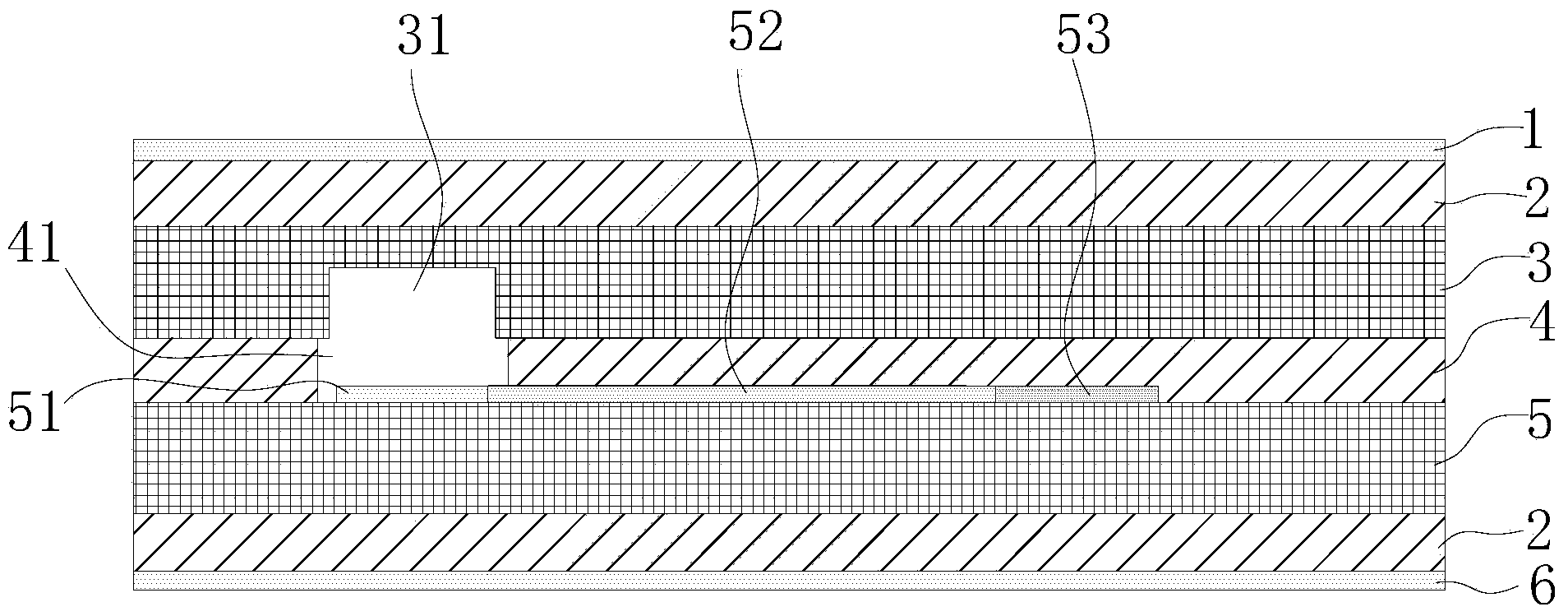
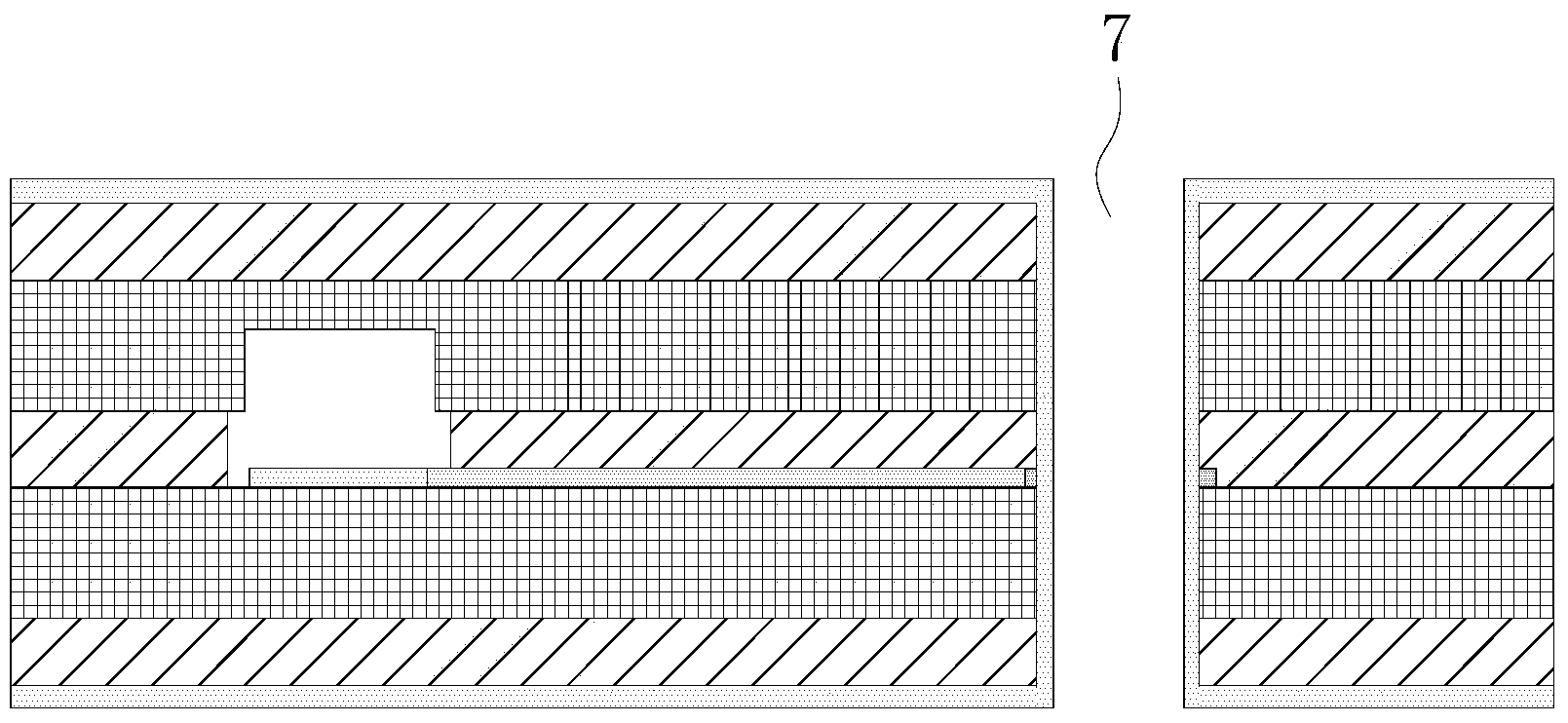
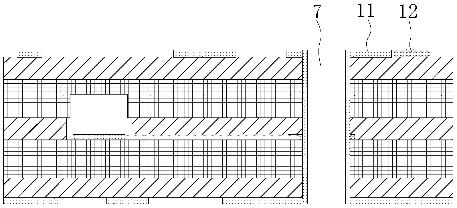
[0021] refer to Figure 1-4 , the present embodiment provides a method for making a deep blind slot in a PCB, which specifically includes the following steps:

[0022] (1) According to the PCB production process of the prior art, the circuit board raw materials are cut to obtain the first core board 5 and the second core board 3, and then the negative film process is used to make the first inner layer circuit on the first core board 5 , making a second inner layer circuit on the second core board 3 . Specifically:

[0023] The first core board 5 and the second core board 3 are firstly subjected to inner layer pre-treatment to remove oxides on the board surface, clean and roughen the board surface. The process is: degreasing→water washing→micro-etching→water washing→pickling→water washing→dry board.

[0024] Then respectively paste the dry film on the first core board 5 and the second core board 3, and sequentially carry out exposure and development, so that the first inner ...


PUM


Abstract

The invention relates to the technical field of printed circuit board (PCB) production, in particular to a method of forming a deep blind groove in a printed circuit board (PCB). The method includes forming a window in a first half cured sheet and pre-forming a groove in a second core plate before pressing, drilling a through groove after manufacturing a resistance welding layer, removing a block above the groove, and obtaining the deep blind groove. The depth of the through groove is reduced, dust can be discharged conveniently, and coked dust clinging to the welding disc of the bottom of the groove is eliminated; the depth of the groove is 2/3 of the thickness of the second core plate, and the unqualified pressing of a block below the bottom of the groove is avoided; the welding disc of the bottom of the groove is exposed after the resistance welding layer is obtained, the oxidation of the welding disc of the bottom of the groove in the air can be reduced, and the welding disc of the bottom of the groove is prevented from being scraped; a first guide wire, a first welding disc and a first metal through hole which are communicated with the welding disc of the bottom of the groove sequentially are arranged, the surface of the welding disc of the bottom of the groove is processed in an electroplating manner, and the problem that since the flowability of liquid drug of the deep blind groove is low and the liquid drug cannot be exchanged, planting omitting of the welding disc of the bottom of the groove occurs is overcome.

Description

technical field [0001] The invention relates to the technical field of circuit board production, in particular to a method for producing deep blind grooves in a PCB. Background technique [0002] PCB is the support of electronic components and the carrier of electrical connections. It is one of the important components of the electronics industry. It is used in almost every kind of electronic equipment, ranging from electronic watches and calculators to computers, communication electronic equipment, and military weapons. system etc. In the PCB, it is usually necessary to make blind slots on it to match the design of the overall circuit. The aspect ratio of the blind slots on the existing PCB is generally ≤0.3:1 (the depth of the blind slot / the width of the blind slot), and the prepreg or the prepreg and the light board are usually opened first, and then pressed and copper deposited Electroplate with the whole board, and then remove the copper foil at the blind slot to expo...

Claims


Application Information

Patent Timeline
Patent Type & Authority Applications(China)
IPC IPC(8): H05K3/46H05K3/42
CPCH05K3/429H05K3/4614
Inventor 刘克敢张军杰韩启龙刘东
Owner SHENZHEN SUNTAK MULTILAYER PCB
Why Eureka
Try Eureka