
A programming control circuit of a programmable chip

A programming control and circuit technology, applied in electrical program control, program control in sequence/logic controllers, etc., can solve the problems of increased cost, limited number of lithography and erasure, and small number of chip programmability. The effect of reducing costs and saving lithography steps

Active Publication Date: 2017-02-22
WUXI ZGMICRO ELECTRONICS CO LTD
View PDF7 Cites 0 Cited by
  • Summary
  • Abstract
  • Description
  • Claims
  • Application Information

AI Technical Summary

Problems solved by technology

This floating gate process undoubtedly increases the cost in the programming process due to the photolithography step, and in some applications, the chip needs to be programmed many times, but the number of photolithography and erasing of the floating gate transistor is limited, making The number of times the chip can be programmed is less

Method used


Image

  • A programming control circuit of a programmable chip
  • A programming control circuit of a programmable chip
  • A programming control circuit of a programmable chip

Examples


Embodiment Construction

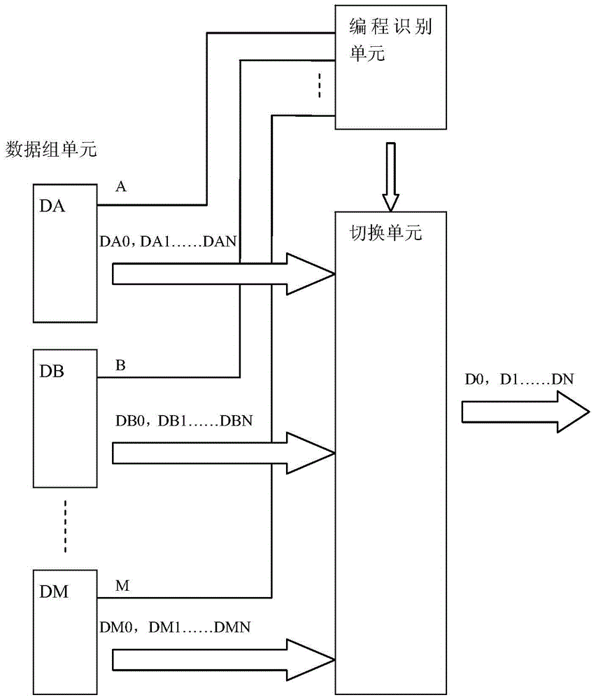
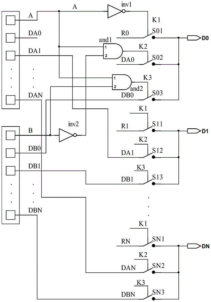
[0013] Such as figure 1 As shown in , it is a functional block diagram of the present invention, including several data group units, which are respectively data group unit DA, data group unit DB...data group unit DM (wherein, M refers to the data group unit selected according to actual needs number, and does not refer to the specific digits obtained in alphabetical order), and also includes a programming identification unit and a switching unit, and each of the data group units includes a flag bit subunit and a plurality of programming data bit subunits (not shown in the figure marked). The programming recognition unit used to identify the number of programming times is respectively connected to the flag subunits in each data group unit DA, DB...DM, that is, the programming recognition unit is connected to the data group unit DA through the flag terminal A The flag bit subunit of the flag bit subunit is connected to the flag bit subunit of the data group unit DB through the f...


PUM


Abstract

The present invention relates to a smart chip, and in particular relates to a chip control program A programmable circuit comprising a plurality of data group unit, program identification unit and the switching unit, each data group unit including a seat unit and a plurality of flag data programming unit seat, the program identification number for identifying the programming unit, are connected with each data group unit flag seat unit, the identification flag signal flag seat unit, and controls the switching unit, the switching unit connection said seat unit program data each data group unit, and under control of the program unit identification, program data corresponding to oN seat unit, an output signal corresponding to program data. The present invention does not require special technology, can achieve the effect of many times programming to save chip photolithography step during production, reduces costs, and need to be increased or decreased according to the number of the data group unit, programmed to achieve several purposes.

Description

technical field [0001] The invention relates to the field of smart chips, in particular to a programming control circuit of a programmable chip. Background technique [0002] In the prior art, a general chip with a programmable function requires a special process to program the chip multiple times. For example, the programming entry of some chips has several floating gate transistors, and additional photolithography steps are required to modify the floating gate transistors during programming. The charge on the gate changes the turn-on threshold voltage of the floating gate transistor, so that the corresponding programming entry always maintains a specific high level or low level state, that is, obtains binary data, thereby realizing the purpose of programming. This floating gate process undoubtedly increases the cost in the programming process due to the photolithography step, and in some applications, the chip needs to be programmed many times, but the number of photolitho...

Claims


Application Information

Patent Timeline
Patent Type & Authority Patents(China)
IPC IPC(8): G05B19/04
CPCG05B19/04
Inventor 王钊
Owner WUXI ZGMICRO ELECTRONICS CO LTD
Learn More