Time sequence determining method and device of integrated circuit chip

A technology of integrated circuits and chips, applied in the field of timing determination of integrated circuit chips, can solve the problem of inability to take into account the speed and accuracy of timing analysis, and achieve the effect of achieving speed and accuracy

Active Publication Date: 2015-02-25
LOONGSON TECH CORP
View PDF3 Cites 12 Cited by
  • Summary
  • Abstract
  • Description
  • Claims
  • Application Information

AI Technical Summary

Problems solved by technology

[0007] The present invention provides a timing determination method and device for an integrated circuit chip to solve the problem in the prior art that the speed and accuracy of timing analysis cannot be taken into account

Method used


Image

  • Time sequence determining method and device of integrated circuit chip
  • Time sequence determining method and device of integrated circuit chip
  • Time sequence determining method and device of integrated circuit chip

Examples


Embodiment Construction

[0035] The technical solution of the present invention will be described in further detail below through specific embodiments and accompanying drawings.

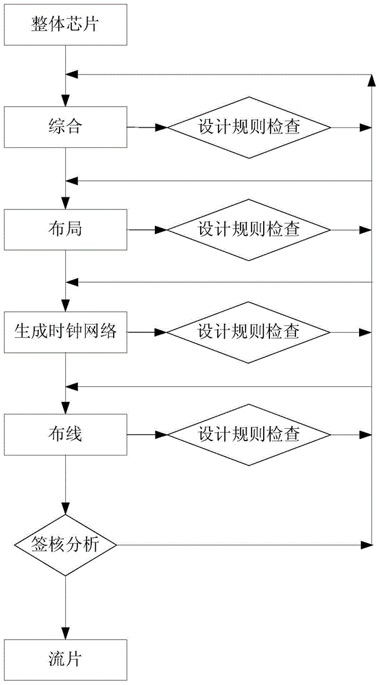
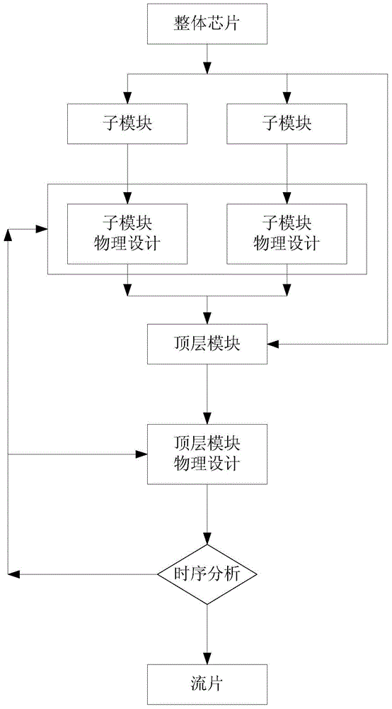
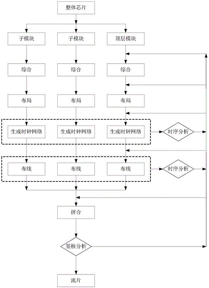
[0036] Figure 4 A schematic flowchart of an embodiment of a method for determining timing of an integrated circuit chip provided by the present invention. Such as Figure 4 As shown, the method may include:

[0037] S401, determine the top-level module included in the integrated circuit chip to be designed and the gate unit included in at least two sub-modules and the position of the gate unit on the integrated circuit chip, and determine the logical connection relationship between the gate units, the gate unit includes a logic unit and sequential units;

[0038]Specifically, when the scale of the integrated circuit is large, the automatic design tool is limited by the scale of the problem that its own algorithm can handle, and cannot handle the physical design problem of a large-scale chip at one time. Therefore, it is ...


PUM


Abstract

The invention provides a time sequence determining method and device of an integrated circuit chip. The time sequence determining method includes subjecting a top module and at least two submodules of an integrated circuit chip to be designed to synthesization, overall arrangement and clock network design generation; extracting a boundary time sequence model according to the clock network of the submodules and the top module; if the boundary time sequence model meets the first time sequence conditions, designing wiring of the submodules and the top module; extracting an electric parameter model according to the wired submodules and the top module; if the electric parameter model meets the second time sequence condition, splicing the submodules and the top module and extracting a transistor model; if the transistor model meets the third time sequence condition, determining the time sequence of the integrated circuit chip. By the time sequence determining method and device, different time sequence models are extracted for different stages of integrated circuit chip design, and balance between speed and accuracy of the time sequence analysis is realized.

Description

technical field [0001] The invention relates to the technical field of power electronics, in particular to a timing determination method and device for an integrated circuit chip. Background technique [0002] The physical design of integrated circuit chips is the process of mapping functional modules described in hardware languages ​​(such as Verilog, VHDL) into layouts through design. figure 1 Flowcharts for traditional physical design methods, such as figure 1 As shown, the traditional physical design method mainly includes five stages of synthesis, layout, clock network generation, routing and signoff analysis. For the first four stages, after each stage is completed, it is necessary to check whether the design meets the corresponding items. If the design rules are not satisfied, return to the previous stage to redesign and optimize, and solve possible problems in the previous stage to reduce the pressure of the final signoff analysis stage. [0003] However, with the ...

Claims


Application Information

Patent Timeline
Patent Type & Authority Applications(China)
IPC IPC(8): G06F17/50
Inventor 王茹肖斌范宝峡
Owner LOONGSON TECH CORP
Why Eureka
Try Eureka