Printed circuit board and mixed surface treatment process thereof

A printed circuit board and surface treatment technology, which is applied in the secondary treatment of printed circuits, reinforcement of conductive patterns, and application of non-metallic protective layers. A large number of problems such as labor of red glue paper, to achieve the effect of reducing costs, high economic value, and reducing the residual rate of blue glue

Active Publication Date: 2015-02-25
KALEX MULTI LAYER CIRCUIT BOARD (ZHONGSHAN) CO LTD
View PDF5 Cites 8 Cited by
  • Summary
  • Abstract
  • Description
  • Claims
  • Application Information

AI Technical Summary

Problems solved by technology

In the surface treatment of tin spraying, the treatment temperature can reach above 260 degrees, and the red glue paper of special material is required, and the cost is high
On the other hand, pasting red adhesive paper on a large area on the board requires a large amount of red adhesive paper and labor, and the positioning accuracy of manual adhesive paper is not high, which is difficult to meet the requirements of high-standard circuit boards

Method used


Image

  • Printed circuit board and mixed surface treatment process thereof
  • Printed circuit board and mixed surface treatment process thereof

Examples


Embodiment 1

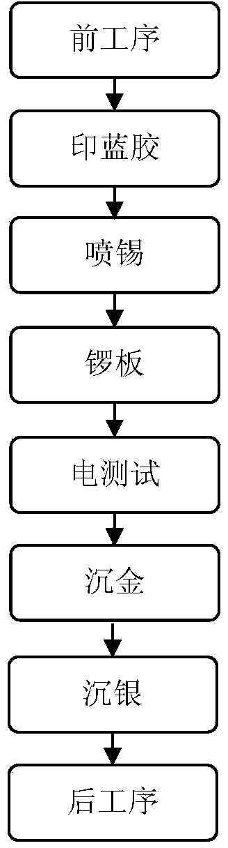
[0043] This embodiment is a mixed surface treatment process for printed circuit boards, including the following processes: pre-process, blue glue printing, tin spraying process, gong board, electrical test, immersion gold, immersion silver and post-process;

[0044] Described printing blue glue operation comprises following process parameter:

[0045] (1) By printing blue glue on the surface of the circuit board, selectively expose the holes that need to be sprayed with tin.

[0046] The main process is as follows: tin-spray hole blue plastic film window is designed so that each side of the light blocking point is 5mil larger than the aperture (1mil=0.0254mm);

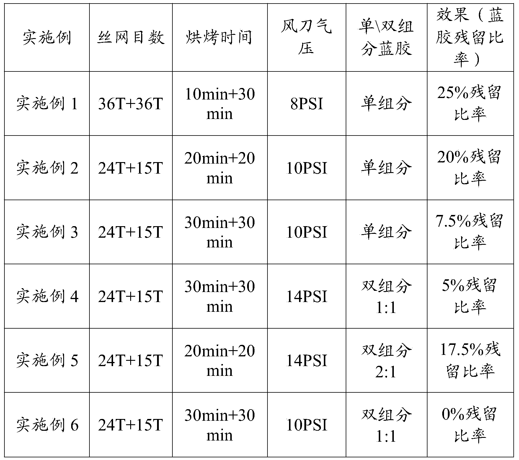
[0047] Use screen printing blue glue twice, use 36T screen for the first time, use 36T screen for the second time; print the component surface first, bake at 135±5°C for 10 minutes after printing, and then print the soldering surface, and then print at 150 Bake at ±5°C for 30 minutes;

[0048] The blue glue is blue g...

Embodiment 2

[0067] The other steps were the same as in Example 1, and the mesh size, baking time and tin-spraying air knife pressure were adjusted.

[0068] Use screen printing blue glue twice, use 24T screen for the first time, and use 15T screen for the second time; print the component surface first, bake at 130°C for 20min after printing, and then print the soldering surface, and then print at 150°C Bake for 20 minutes; use 10PSI air pressure for tin spraying air knife.

[0069] The blue glue is the blue glue B of SD-2955 model.

[0070] Result: 40 circuit boards were tested, and there were blue glue in 8 holes in all inspections, and the residual ratio of blue glue in the holes was 20%.

Embodiment 3

[0072] The other steps were the same as in Example 1, and the mesh size, baking time and tin-spraying air knife pressure were adjusted.

[0073] Use screen printing blue glue twice, use 24T screen for the first time, and use 15T screen for the second time; print the component surface first, bake at 130°C for 30 minutes after printing, then print the soldering surface, and then print at 150°C Bake for 30 minutes; use 10PSI air pressure for tin spraying air knife.

[0074] The blue glue is blue glue A of SD-2954 model.

[0075] Results: 40 circuit boards were tested, and there were blue glue in the holes of 3 of them, and the residual ratio of blue glue in the holes was 7.5%.


PUM


Abstract

The invention discloses a printed circuit board and a mixed surface treatment process of the printed circuit board. The mixed surface treatment process comprises the following procedures of the previous procedure, blue glue printing, the tin spraying procedure, the plate milling procedure, electric tests, gold deposition, silver deposition and the subsequent procedure, wherein the blue glue is printed in a silk-screen printing mode, the silk screen has the specification of 15T or 24T or 36T; an element face is first printed with the blue glue, then, baking is performed for 5 min to15 min at the temperature of 135+ / -5 DEG C; a welded face is printed with the blue glue, then, baking is performed for 25 min to 35 min at the temperature of 150+ / -5 DEG C. According to the printed circuit board and the mixed surface treatment process of the printed circuit board, the blue glue technology is creatively used for forming a selective tin spraying protection layer; particularly blue glue with two different models is used in cooperation, and the blue glue residual rate on the plate faces is reduced; the various surface treatment processes are used for the same circuit board, and therefore various product requirements can be met; cost can also be reduced, and very high economic value is achieved.

Description

technical field [0001] The invention relates to the technical field of printed circuit boards, in particular to a printed circuit board and its mixed surface treatment process. Background technique [0002] The surface treatment process of the circuit board mainly plays the role of conductivity, welding, anti-oxidation and corrosion resistance. According to different application requirements, common surface treatment processes include: tin spraying (HAL), organic coating (OSP), immersion gold (Immersion Au), immersion silver (Immersion Silver) and immersion tin (Immersion Tin). Usually circuit board products mainly adopt a single surface treatment process. For circuit boards with a variety of surface treatments, the common ones are circuit boards with gold fingers. The gold fingers use immersion gold technology, and other parts use another surface technology, such as immersion tin, tin spraying, etc. [0003] In the prior art, red plastic paper is used as the resist layer ...

Claims


Application Information

Patent Timeline
Patent Type & Authority Applications(China)
IPC IPC(8): H05K3/22H05K3/28H05K3/24
Inventor 戴匡
Owner KALEX MULTI LAYER CIRCUIT BOARD (ZHONGSHAN) CO LTD
Why Eureka
Try Eureka