Photoresist removing method

A photoresist and hard shell technology, which is applied in photosensitive material processing, electrical components, semiconductor/solid-state device manufacturing, etc., can solve problems such as polymer impurity defects, photoresist bubbling rupture, etc., to improve deglue ability, The effect of speeding up the degumming rate and improving product yield and quality

Inactive Publication Date: 2015-03-04
SHANGHAI HUALI MICROELECTRONICS CORP
View PDF7 Cites 12 Cited by
  • Summary
  • Abstract
  • Description
  • Claims
  • Application Information

AI Technical Summary

Problems solved by technology

[0009] In order to solve the above-mentioned problems in the prior art, the present invention provides a photoresist removal method to solve the technical problems of photoresist bubbling and polymer impurity defects during deglue removal in the prior art

Method used


Image

  • Photoresist removing method
  • Photoresist removing method

Examples


no. 1 example

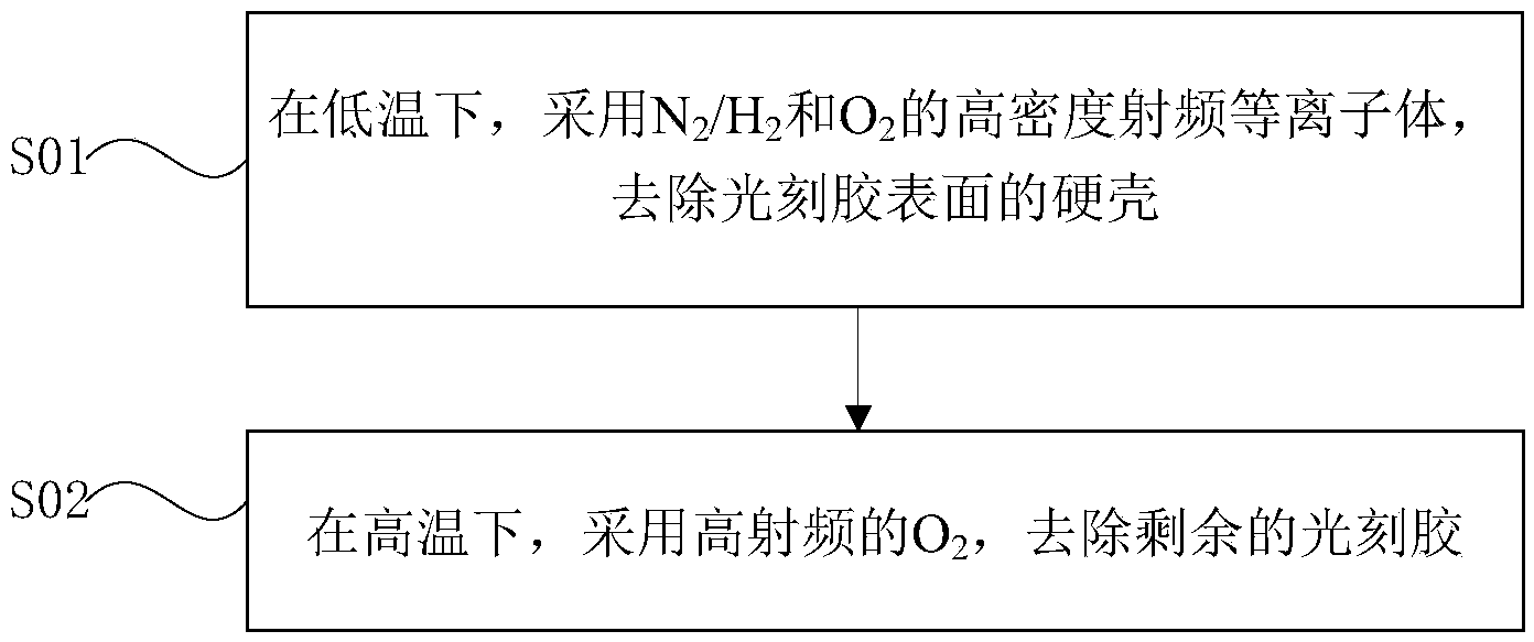
[0027] see figure 2 , the photoresist removal method in this embodiment, the photoresist surface has a hard shell after ion implantation, which includes the following two steps:

[0028] Step S01, at low temperature, using N 2 / H 2 and O 2 The high-density radio frequency plasma removes the hard shell on the surface of the photoresist.

[0029] The "low temperature" described in this step is much lower than the crust removal temperature in the prior art. Generally, the crust removal reaction temperature in the prior art is 200-300°C, as long as it is much lower than the reaction temperature, and it is not easy to make the The temperature at which the volatile solvent in the glue emits is within the protection scope of the present invention, preferably 50-80° C., which can not only ensure the reaction rate, but also prevent the volatile solvent from excessively dispersing.

[0030] Since this step adopts a low temperature reaction temperature, in order to ensure the effect...


PUM


Abstract

The present invention discloses a photoresist removing method. According to the photoresist removing method, with the fractional temperature control photoresist removing process, the low temperature is maintained during the photoresist surface hard shell removing process, such that the photoresist polymer impurity generation caused by the emission of the volatile solvent in the photoresist, and the high density radio frequency reaction gas is adopted so as to completely react with the hard shell; and during the residual photoresist removing process, the high temperature is maintained, and the high radio frequency reaction gas is adopted so as to accelerate the photoresist removing rate and improve the photoresist removing ability, such that the product yield and the product quality are increased through the photoresist removing method of the present invention.

Description

technical field [0001] The invention relates to the technical field of semiconductor manufacturing, in particular to a method for removing photoresist after ion implantation. Background technique [0002] When designing semiconductor devices, considering the device performance requirements, it is necessary to perform ion implantation on specific regions to meet the different functional requirements of various devices. After high-energy ion implantation of the wafer coated with photoresist, a hard crust with a certain thickness will be formed on the surface of the area covered by the photoresist. figure 1 is a schematic diagram of the photoresist structure after high-energy ion implantation, such as figure 1 As shown, after the photoresist covered on the substrate 11 undergoes a high-energy ion implantation process, the exposed part forms a hard shell 13, and the inside of the shell 13 is also wrapped with a layer that has not been irradiated by high-energy ions (that is, ha...

Claims


Application Information

Patent Timeline
Patent Type & Authority Applications(China)
IPC IPC(8): G03F7/42H01L21/311
Inventor 高慧慧秦伟李程杨渝书
Owner SHANGHAI HUALI MICROELECTRONICS CORP
Why Eureka
Try Eureka