Method for producing touch screen sensor in gravure micro transfer printing way

A touch screen sensor, pad printing technology, applied in the input/output process of instruments, data processing, electrical digital data processing, etc., can solve the problems of high material cost, waste of materials, water and electricity consumption, slow laser efficiency, etc. The effect of precision and alignment accuracy, elimination of environmental pollution, and cost savings

Active Publication Date: 2015-03-04
深圳市瑞捷恩科技有限公司
View PDF5 Cites 7 Cited by
  • Summary
  • Abstract
  • Description
  • Claims
  • Application Information

AI Technical Summary

Problems solved by technology

However, the yellow light process has very high requirements for the configuration of the gluing machine and the exposure machine, and the equipment cost has always been high; in addition, the parallel light exposure requires a special mask for each layer structure, and the material cost is relatively high; after exposure, development and other wastes are required. Extensive material and water consumption
The disadvantages of maskless lithography and laser laser are that the laser efficiency is slow, the energy is not easy to control, and it is easy to form short circuits and other defects.
The silk screen printing process is mainly used in the formation of some patterns such as Film that do not require high precision. It has low precision and slow efficiency, and cannot complete the production of high-precision and high-resolution structures.
Although the inkjet printing method does not require exposure and development processes, which saves material and equipment costs, it has high requirements for materials and inkjet printers, and problems such as material diffusion and resolution on the substrate have not been well resolved.

Method used


Image

  • Method for producing touch screen sensor in gravure micro transfer printing way
  • Method for producing touch screen sensor in gravure micro transfer printing way

Examples


Embodiment Construction

[0023] Embodiments of the present invention will now be described with reference to the drawings, in which like reference numerals represent like elements. As mentioned above, a method for fabricating a touch screen by gravure micro pad printing is provided. Such as figure 1 and 2 as shown,

[0024] A method for producing a touch screen sensor by gravure micro pad printing, comprising the steps of:

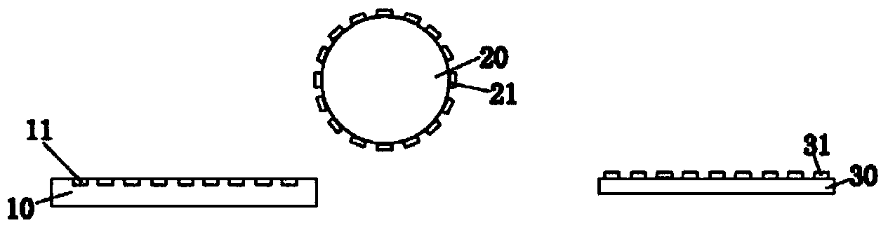
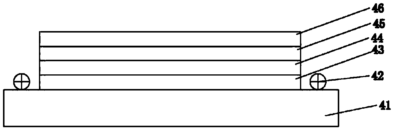
[0025] Gravure 10 design steps: According to the single-grain size drawing of the touch screen sensor, such as 3.5-inch, 4-inch, 5-inch, 7-inch drawing and other size drawing, according to the size of the substrate material such as glass Glass or film Film, in the Typesetting on the electronic graphic file; then follow the touch screen sensor structure graphic file, such as BM (Black matrix), various color inks, ITO electrodes, OC (Overcoater) insulating layer, metal molybdenum aluminum molybdenum (MOALMO) electrodes, metal Cu or silver Slurry electrode, OC (Overcoater) protec...


PUM


Abstract

The invention discloses a method for producing a touch screen sensor in a gravure micro transfer printing way. The method comprises the steps of designing and producing a gravure, loading and pre-positioning a transfer printing roller, loading and positioning the gravure, aligning the gravure and a transfer printing substrate, filling grooves of the gravure and collecting ink, a micro transfer printing, to be specific: adjusting the clearance and pressure between the transfer printing roller and the gravure and between the transfer printing roller and the transfer printing substrate after the starting point position of the transfer printing roller on the gravure and the transfer printing substrate is adjusted; under the action of adhesion force of the transfer printing roller, adhering a transfer printing material in the groove of the gravure, and starting a heating system; transfer-printing the transfer printing material on the roller to an end point while the viscosity of the transfer printing material is reduced after the roller reaches a starting point of the substrate, injecting cooling water into the roller, cooling the roller, discharging the cooling water after the roller is cooled to certain temperature, and carrying out the next transfer printing; forming the touch screen sensor structure. By adopting the method, the production of all touch screen sensors in different sizes and with different substrates can be satisfied, the precision is high, the efficiency is high, and the environmental pollution is avoided.

Description

technical field [0001] The invention relates to a method for manufacturing a touch screen sensor by gravure micro pad printing. Background technique [0002] The touch screen Touch Sensor is divided into two types according to the material, Film and Glass material. Film-type sensors are generally divided into single-layer and double-layer structures. The film structure of each layer is generally ITO Pattern, and the edge Ag paste is routed. Traditional Glass Sensor is divided into single-layer multi-point, DITO, SITO and many other structures. At this stage, the mainstream is OGS structure, and the structure and process sequence are different. [0003] Based on the evolution of the touch screen structure, the production methods of the Touch Panel are also emerging one after another. Especially for the forming part of the pattern circuit, the current method with the highest precision and resolution is the parallel light exposure process: under the action of g, h, and i-band...

Claims


Application Information

Patent Timeline
Patent Type & Authority Applications(China)
IPC IPC(8): G06F3/044
CPCG06F3/044
Inventor 赵跃杜德海
Owner 深圳市瑞捷恩科技有限公司
Why Eureka
Try Eureka