Solder ball and electronic member

A technology of electronic components and solder balls, which is applied in the direction of electrical components, electrical components assembled printed circuits, printed circuits, etc., to achieve excellent thermal fatigue characteristics, good drop impact resistance, and the effect of suppressing porosity

Inactive Publication Date: 2015-03-04
NIPPON STEEL CHEM &MATERIAL CO LTD +1
View PDF12 Cites 7 Cited by
  • Summary
  • Abstract
  • Description
  • Claims
  • Application Information

AI Technical Summary

Problems solved by technology

[0006] However, since Ag is expensive, it is not desirable to add about 3% by mass, and if Ag is added at about 3% by mass, the needle-shaped Ag will 3 A large amount of Sn is precipitated in Sn, and when the flux used in the above-mentioned temporary bonding is vaporized by the heat of reflow soldering, the gas is absorbed by the needle-shaped Ag. 3 Sn trapping, pores (voids, void) caused by air bubbles are easily formed near the bonding interface

Method used


Image

  • Solder ball and electronic member
  • Solder ball and electronic member
  • Solder ball and electronic member

Examples


Embodiment

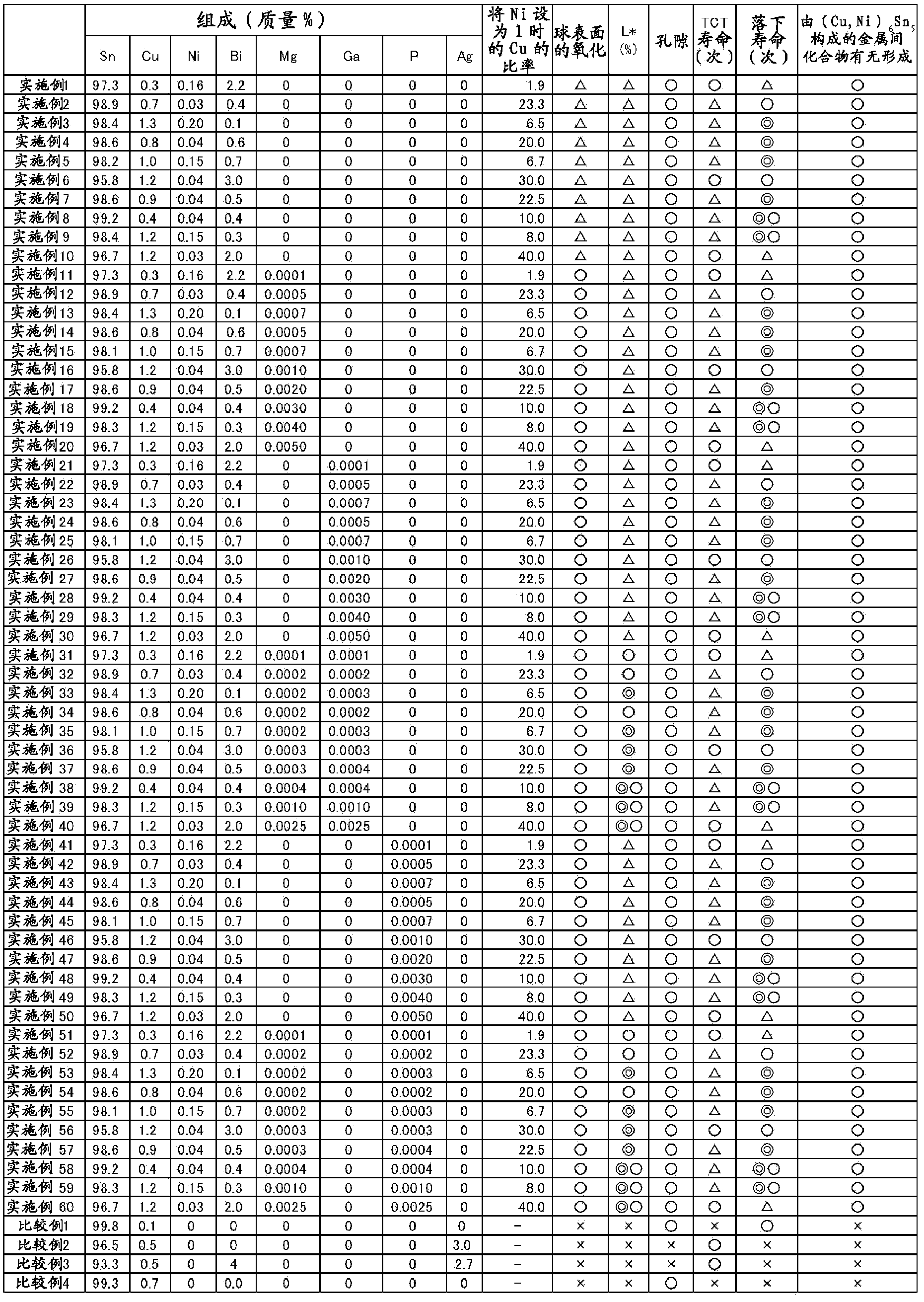
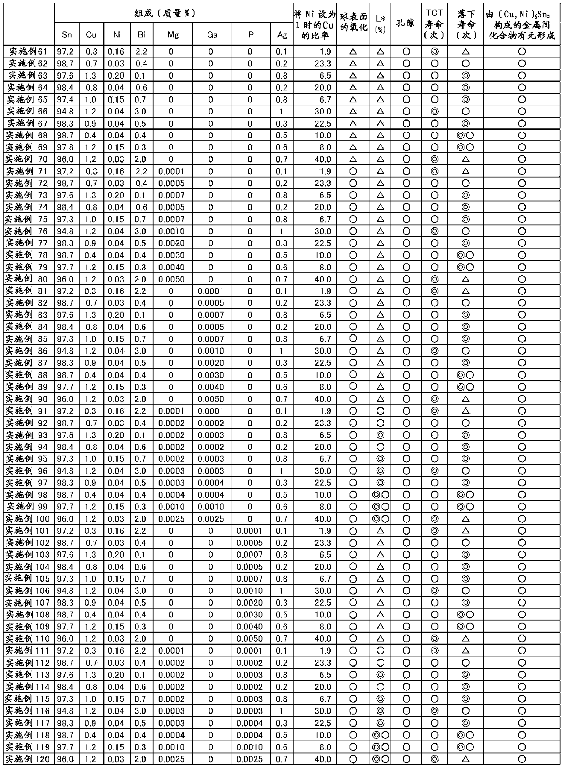
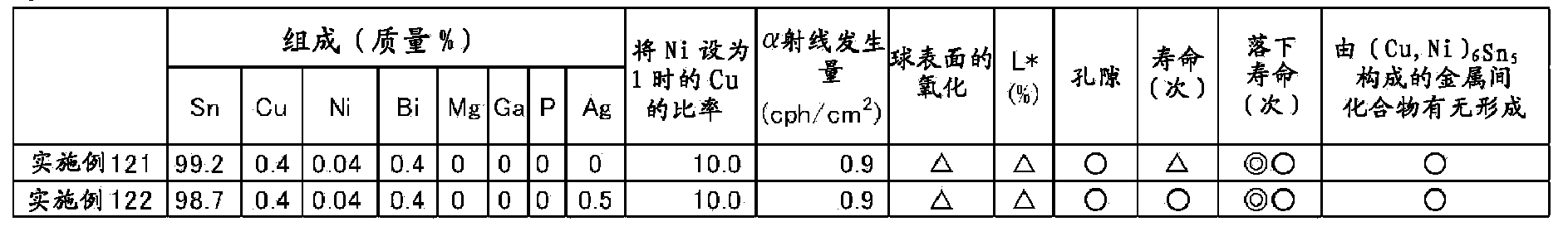
[0065] The composition of the solder alloy used as solder balls was changed, and the ball surface of each solder ball, the presence or absence of voids, thermal fatigue characteristics (TCT characteristics), and drop impact resistance characteristics (drop characteristics) were investigated. Here, a predetermined amount of Cu and Ni are heated to 275[°C] in a high-frequency melting furnace in advance to form a master alloy, and after producing a Cu-Ni-based master alloy, add Bi etc. This master alloy (Cu-Ni-based master alloy) was added to the Sn-Bi-based raw material to produce a raw material. Next, this raw material was placed in a graphite crucible, heated to 275[° C.] in a high-frequency melting furnace to be melted, and then cooled to obtain a solder alloy for semiconductor mounting.

[0066] Thereafter, the solder alloy was made into a wire rod having a wire diameter of 20 [μm]. This wire rod was cut into a constant volume at a length of 6.83 [mm], heated and melted aga...


PUM

PropertyMeasurementUnit
lengthaaaaaaaaaa

Abstract

Provided are: a solder ball which is capable of achieving excellent thermal fatigue characteristics and good drop impact resistance characteristics, while suppressing generation of voids in a joined part; and an electronic member which uses this solder ball. This solder ball is formed of an Sn-Bi system alloy, which is mainly composed of Sn and contains 0.3-2.0% by mass of Cu, 0.01-0.2% by mass of Ni and 0.1-3.0% by mass of Bi, and is configured such that an intermetallic compound composed of (Cu, Ni)6Sn5 is formed in the Sn-Bi system alloy. Consequently, this solder ball is capable of achieving excellent thermal fatigue characteristics and good drop impact resistance characteristics, while suppressing generation of voids in a joined part in cases where this solder ball is joined to an electrode.

Description

technical field [0001] The present invention relates to a solder ball (solder ball, Solder ball) for mounting a semiconductor, and an electronic component using the solder ball. Background technique [0002] Electronic components are mounted on a printed wiring board or the like. The mounting of electronic components is generally carried out by the following method called the so-called reflow method: solder balls for semiconductor mounting (hereinafter referred to as "solder balls") are placed between printed wiring boards, etc., and electronic components. ".) and flux (Flux), heat the entire printed wiring board to melt the above-mentioned solder balls, and then cool the board to room temperature to solidify the solder balls, thereby ensuring firm solder joints section (also referred to only as the junction section). [0003] When an electronic device incorporating a printed circuit board or the like is operated, heat is generated inside the electronic device due to an el...

Claims


Application Information

Patent Timeline
Patent Type & Authority Applications(China)
IPC IPC(8): B23K35/26C22C13/02H05K3/34
CPCC22C13/00B23K35/26H05K3/3463C22C13/02H05K2203/041B23K2101/36B23K35/0244B23K35/262B23K1/0016H05K1/181H05K3/34H05K3/3457
Inventor 寺岛晋一小林孝之田中将元木村胜一佐川忠礼
Owner NIPPON STEEL CHEM &MATERIAL CO LTD
Why Eureka
Try Eureka