LED (light emitting diode) epitaxial layer structure and growth method thereof

A technology of epitaxial structure and growth method, applied in electrical components, circuits, semiconductor devices, etc., can solve the problems of LED device luminous efficiency, low carrier recombination efficiency, large lattice mismatch, etc.

Active Publication Date: 2015-03-11
XIANGNENG HUALEI OPTOELECTRONICS
View PDF4 Cites 20 Cited by
  • Summary
  • Abstract
  • Description
  • Claims
  • Application Information

AI Technical Summary

Problems solved by technology

[0003] LED is a PN node, mainly divided into N-type GaN, light-emitting layer, and P-type GaN. The light-emitting layer is generally a superlattice composed of InGaN/GaN pairs. There is a large lattice mismatch between InGaN materials and GaN mat...

Method used


Image

  • LED (light emitting diode) epitaxial layer structure and growth method thereof
  • LED (light emitting diode) epitaxial layer structure and growth method thereof
  • LED (light emitting diode) epitaxial layer structure and growth method thereof

Examples


Embodiment 1

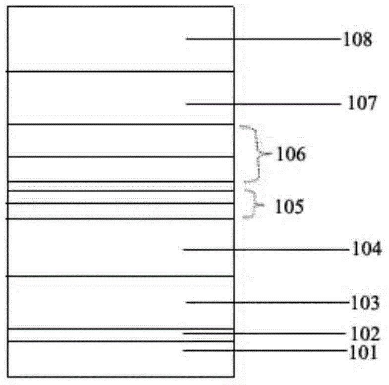
[0041] Such as figure 1 As shown, this embodiment provides an LED epitaxial structure, which includes sequentially from bottom to top:

[0042] A sapphire substrate 101, the sapphire substrate in this embodiment is a C-Plane sapphire substrate. However, it should be noted that the present invention does not limit the type and parameters of the sapphire substrate provided, such as thickness, diameter, crystal orientation, warpage, etc., and the specific parameters are determined according to specific design requirements.

[0043] A low-temperature buffer layer 102 located on the sapphire substrate 101;

[0044] a high-temperature GaN layer 103 located on the low-temperature buffer layer 102;

[0045] a high-temperature N-type GaN layer 104 located on the high-temperature GaN layer 103;

[0046] The transition layer 105 is located on the high-temperature N-type GaN layer 104, wherein the transition layer 105 is a transition layer in which Si3N4 / GaN superlattice layers and und...

Embodiment 2

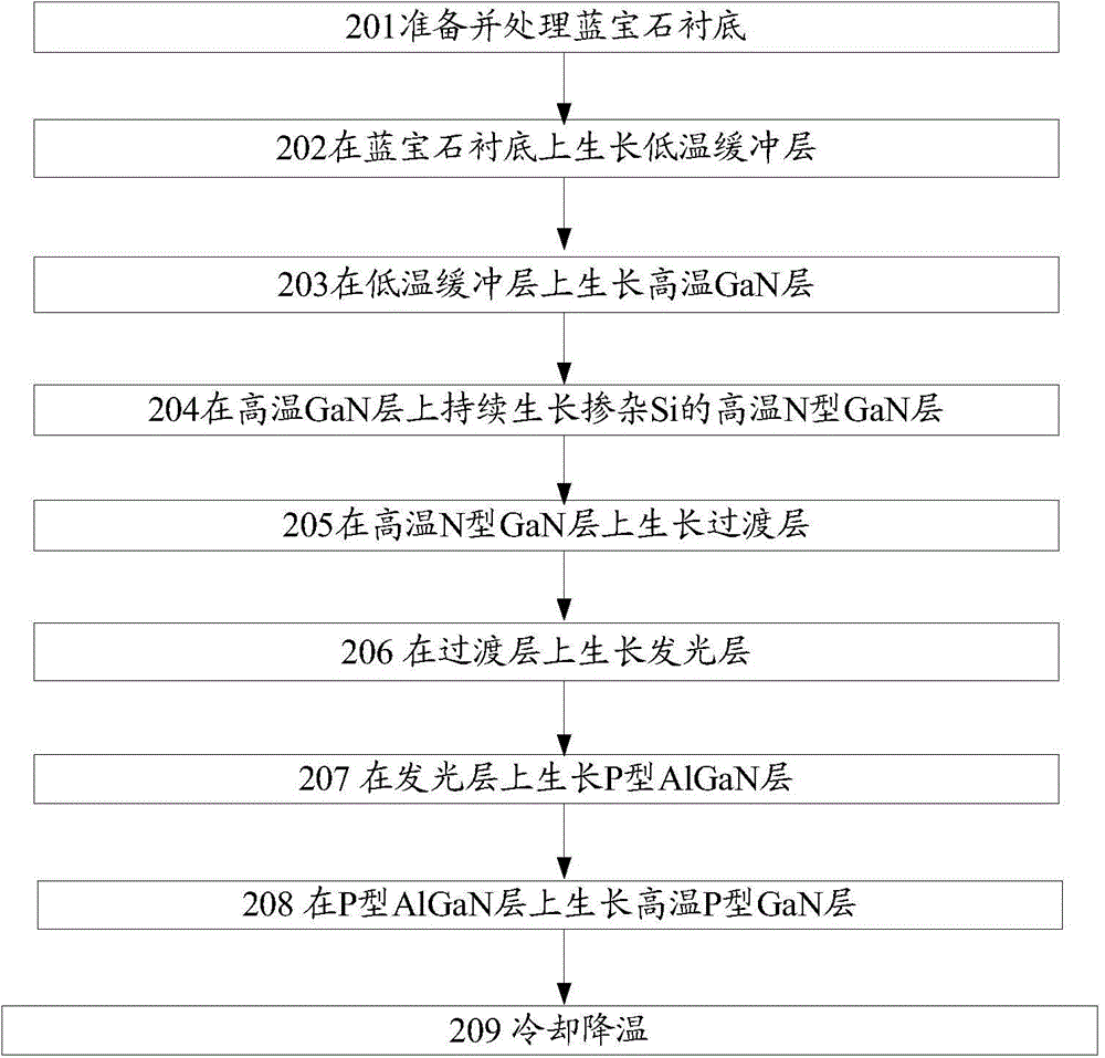
[0064] In this embodiment, the LED epitaxial structure is grown according to the following steps:

[0065] 1) Treat the sapphire substrate at 1100°C for 8 minutes under a hydrogen atmosphere with the reaction chamber pressure maintained at 100mbar;

[0066] 2) Lower the temperature to 600°C, maintain the pressure of the reaction chamber at 500mbar, and grow a low-temperature buffer layer GaN with a thickness of 35nm on the sapphire substrate;

[0067] 3) Raise the temperature to 1100°C, maintain the pressure of the reaction chamber at 250mbar, and continue to grow a 3μm undoped GaN layer;

[0068] 4) The temperature is 1100°C, the pressure is 300mbar, 250sccm TMGa, 60000sccmNH3 and 30sccmSiH4 are introduced, the growth time is 2000s, and the N-type GaN layer doped with Si is continuously grown, and the Si doping concentration is 7×10 18 , the total thickness is controlled at 3 μm;

[0069] 5) Lower the temperature to 800°C, maintain the pressure in the reaction chamber at 30...


PUM

PropertyMeasurementUnit
Thicknessaaaaaaaaaa
Thicknessaaaaaaaaaa
Thicknessaaaaaaaaaa

Abstract

The invention discloses an LED (light emitting diode) epitaxial layer structure. The LED epitaxial layer structure comprises a sapphire substrate, a low temperature buffer layer located on the sapphire substrate, a high temperature GaN layer located above the low temperature buffer layer, a high temperature N type GaN layer located above the high temperature GaN layer, a transition layer located above the high temperature N type GaN layer, a luminous layer arranged above the transition layer, a P type AlGaN layer located above the luminous layer and a high temperature P type GaN layer located above the P type AlGaN layer, wherein the transition layer is formed by alternately arranging Si3N4/GaN superlattice layers and non-doped GaN layers, the thickness of the transition layer ranges from 30nm to 120nm, and the luminous layer comprises InxGa(1-x)N layers doped with In and non-dopted GaN layers, which are alternately arranged. The invention further discloses a growth method of the LED epitaxial layer structure. The LED epitaxial layer structure reduces stress between the high temperature N type GaN layer and the luminous layer.

Description

technical field [0001] This application relates to the manufacturing technology of LED epitaxial structure, more specifically, relates to an LED epitaxial structure and its growth method in which a layer of Si3N4 / GaN superlattice is inserted between the N layer and the light emitting layer. Background technique [0002] At present, the domestic MOCVD epitaxial growth technology covers about 70% of the LED industry technology. How to grow better epitaxial wafers has been paid more and more attention. The key to the epitaxial technology is how to improve the recombination efficiency of quantum wells. Macroscopically, it is how to improve the light-emitting layer. light efficiency; [0003] LED is a PN node, mainly divided into N-type GaN, light-emitting layer, and P-type GaN. The light-emitting layer is generally a superlattice composed of InGaN / GaN pairs. There is a large lattice mismatch between InGaN materials and GaN materials. , resulting in a large stress between the li...

Claims


Application Information

Patent Timeline
IPC IPC(8): H01L33/06H01L33/00
CPCH01L33/005H01L33/0075H01L33/02H01L33/06H01L2933/0008H01L2933/0066
Inventor 张宇苗振林牛凤娟
Owner XIANGNENG HUALEI OPTOELECTRONICS
Why Eureka
Try Eureka