Implementation method of programmable general digital quantity I/O signal conditioning

A technology of signal conditioning and implementation method, applied in the direction of logic circuits using optoelectronic devices, logic circuits using specific components, etc., can solve the problems of increased material resources, time-consuming, and cannot be completed at the same time, and achieves low cost, simple and fast control. , to achieve the effect of isolation

Inactive Publication Date: 2015-03-11
NO 771 INST OF NO 9 RES INST CHINA AEROSPACE SCI & TECH
View PDF5 Cites 7 Cited by
  • Summary
  • Abstract
  • Description
  • Claims
  • Application Information

AI Technical Summary

Problems solved by technology

However, the current solutions all have certain disadvantages, or they cannot simultaneously complete the signal drive for multi-voltage, multi-flow, multi-form loads and the reception of multi-voltage, multi-flow, multi-form source signals in the same design, or It is necessary to re-solder the connection, temporarily design a new circuit board, or open the case after the machine is powered off, and re-adjust the jumper
This is a method that consumes time, manpower, and material resources and increases the probability of error due to human factors

Method used


Image

  • Implementation method of programmable general digital quantity I/O signal conditioning
  • Implementation method of programmable general digital quantity I/O signal conditioning
  • Implementation method of programmable general digital quantity I/O signal conditioning

Examples


Embodiment 1

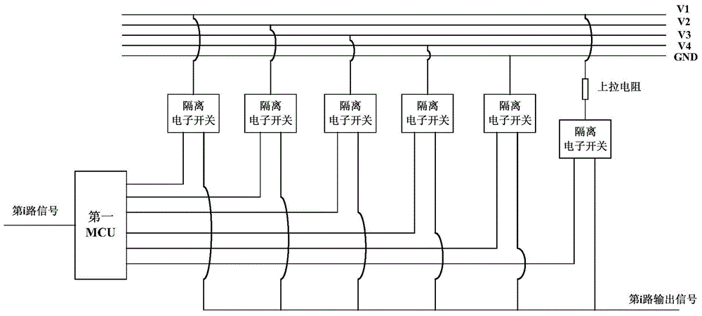
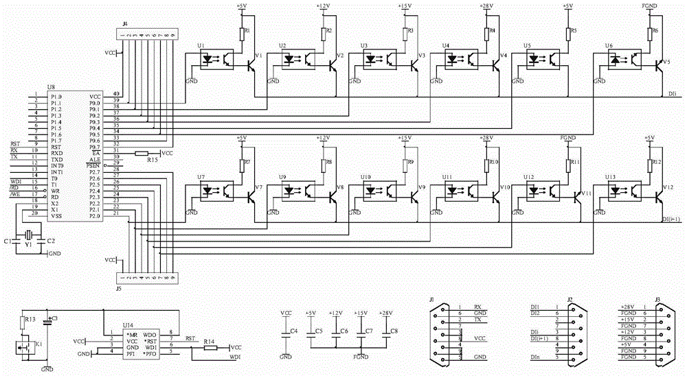
[0039] Such as image 3 As shown, the design circuit in this embodiment is composed of a first MCU processing unit and an isolated electronic switch conditioning circuit, wherein the isolated electronic switch conditioning circuit is composed of N conditioning output signal channels, and each channel is composed of six groups of different isolation channels. Voltage isolating switch circuit.

[0040] Such as image 3 As shown, in the signal output channel, each group of output channels is composed of six groups of isolation switch circuits connected with different isolation voltages, specifically: in the output channel DO(i), resistor R1, optocoupler U1 and transistor V1 constitute The first set of isolating switch circuit is established, the isolation voltage is 5V, where the collector of optocoupler U1 is connected to one end of resistor R1, the other end of resistor R1 is connected to 5V power supply, the emitter of optocoupler U1 is connected to the base of triode V1, and...

Embodiment 2

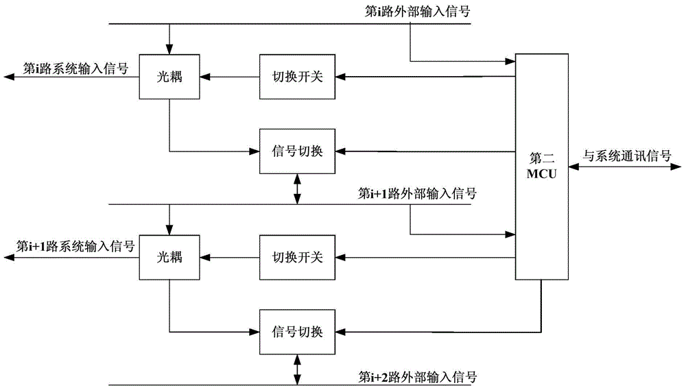
[0051] Such as Figure 4 As shown, the design circuit in the embodiment is composed of a second MCU processing unit, a switching circuit, a signal switching circuit and an isolation optocoupler.

[0052] Such as Figure 4 As shown, in the first DO(i) input channel, the switching circuit includes resistors R24, R25, R26, R27, R16, R17, R18, R19 and transistors V13, V14, V15, V16; among them, the resistors R24, R25 One end of R26 and R27 is connected to the cathode of the light-emitting diode of optocoupler U16, the other end of resistors R24, R25, R26 and R27 are respectively connected to the collectors of transistors V16, V15, V14 and V13, and the collectors of transistors V13, V14, V15 and V16 The emitters are commonly connected to the anode of the output terminal of the optocoupler U17 and the anode of the output terminal of the optocoupler U18, the bases of the transistors V13, V14, V15 and V16 are respectively connected to one end of the resistors R16, R17, R18 and R19, a...


PUM


Abstract

The invention discloses an implementation method of a programmable general digital quantity I / O signal conditioning. The method comprises the following steps: for an output signal conditioning in a general digital signal, adopting a first MCU processing unit and an isolating electronic switching circuit to implement a both-way flow channel of an external output signal; for the access of a plurality of different voltage digital signals, implementing the output conditionings of different voltages by controlling the isolating electronic switching circuit through the first MCU processing unit; for a multiform load signal-point output digital signal, adopting a Darlington circuit to improve the output gain so as to increase output driving capacity; and adopting the first MCU processing unit to control on-off of the isolating electronic switching circuits at different channels so as to implement the conditioning on a two-point differential output signal; for an input signal conditioning in the general digital signal, adopting a second MUC control unit to control a selector switching circuit to implement the selection of the single-point digital signal input or the two-point digital input signal, wherein the voltages, which automatically acquire the external input signal, of the second MCU control unit automatically select different driving channels to control the input signal conditionings in different current directions.

Description

technical field [0001] The invention belongs to the field of computer applications, and in particular relates to a method for realizing the conditioning of programmable general digital I / O signals. Background technique [0002] The general conditioning of digital I / O signals has been a problem that has plagued simulation test design for many years. However, the current solutions all have certain disadvantages, or they cannot simultaneously complete the signal drive for multi-voltage, multi-flow, multi-form loads and the reception of multi-voltage, multi-flow, multi-form source signals in the same design, or It is necessary to re-solder the connection, temporarily design a new circuit board, or open the case after the machine is powered off, and re-adjust the jumper. This is a method that consumes time, manpower, and material resources and increases the probability of error due to human factors. Contents of the invention [0003] The purpose of the present invention is to...

Claims


Application Information

Patent Timeline
Patent Type & Authority Applications(China)
IPC IPC(8): H03K19/14
Inventor 王楠苏理段晓飞王琛窦森
Owner NO 771 INST OF NO 9 RES INST CHINA AEROSPACE SCI & TECH
Why Eureka
Try Eureka