
Touch panel with conductive protection layer and manufacturing method thereof

A conductive protective layer, touch panel technology, applied in electrical digital data processing, data processing input/output process, instruments, etc. In order to achieve the effect of good isolation buffer protection, improve stability and avoid fracturing

Inactive Publication Date: 2015-03-25
TPK TOUCH SOLUTIONS (XIAMEN) INC
View PDF12 Cites 6 Cited by
  • Summary
  • Abstract
  • Description
  • Claims
  • Application Information

AI Technical Summary

Problems solved by technology

However, when forming the above-mentioned touch panel, since the signal lead layer is bonded to the printed circuit board through conductive glue, the signal leads on the signal lead layer may be crushed during the lamination process, which may cause the electrode layer to be separated from the printed circuit board. Problems such as the failure of the board to conduct, affect the stability of the electrical connection between the signal lead layer and the flexible circuit board in the touch panel, and then affect the yield of the product

Method used


Image

  • Touch panel with conductive protection layer and manufacturing method thereof
  • Touch panel with conductive protection layer and manufacturing method thereof
  • Touch panel with conductive protection layer and manufacturing method thereof

Examples


Embodiment Construction

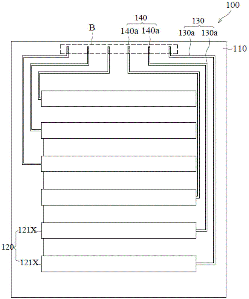
[0021] Several different embodiments are provided due to different features of the invention. The specific components and arrangements in the present invention are for simplicity, but the present invention is not limited to these embodiments. For example, a description of forming a first component over a second component may include embodiments in which the first component is in direct contact with the second component, as well as having an additional component formed between the first component and the second component such that the second component An embodiment in which one component is not in direct contact with a second component. In addition, for the sake of brevity, the present invention is represented by repeated component symbols and / or letters in different examples, but it does not mean that there is a specific relationship between the various embodiments and / or structures.

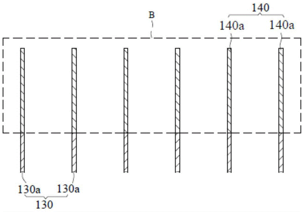
[0022] figure 1 A top view of the touch panel 100 according to an embodiment of the presen...


PUM

PropertyMeasurementUnit
Thicknessaaaaaaaaaa

Abstract

The invention provides a touch panel with a conductive protection layer. The touch panel with the conductive protection layer is characterized in that the touch panel comprises a substrate, a sensing electrode layer, a signal lead layer and a conductive protection layer, wherein a joint area is defined on the substrate, the sensing electrode layer is arranged on the substrate, the signal lead layer is arranged on the substrate and comprises multiple signal leads, one end of each signal lead is electrically connected to the sensing electrode layer, the other end of each signal lead is gathered to the joint area, the conductive protection layer comprises multiple conductive blocks, each conductive block is located on the corresponding signal lead in the joint area, and the signal leads are electrically insulated with one another. The invention further provides a manufacturing method of the touch panel with the conductive protection layer. The touch panel and the manufacturing method aim to solve the problem that signal leads are prone to fracturing when being attached to a flexible printed circuit in the prior art, and the product yield is increased.

Description

technical field [0001] The present invention relates to touch technology, and in particular to a touch panel with a conductive protective layer and a manufacturing method thereof. Background technique [0002] With the evolution of touch technology (Touch control), touch panels have been widely used in various consumer electronic devices, such as: smart phones, tablet computers, cameras, e-books, MP3 players and other portable electronic devices. products, or display screens applied to operator control equipment. [0003] A touch panel generally includes a substrate, an electrode layer, and a signal lead layer electrically connecting the electrode layer to a printed circuit board. However, when forming the above-mentioned touch panel, since the signal lead layer is bonded to the printed circuit board through conductive glue, the signal leads on the signal lead layer may be cracked during the lamination process, which may cause the electrode layer to be separated from the pr...

Claims


Application Information

Patent Timeline
IPC IPC(8): G06F3/041
CPCG06F3/0412G06F2203/04103G06F2203/04111
Inventor 袁琼张专元黄萍萍
Owner TPK TOUCH SOLUTIONS (XIAMEN) INC
Learn More