Copper interconnection structure and method for manufacturing same

A technology of copper interconnection structure and manufacturing method, applied in semiconductor/solid-state device manufacturing, electrical components, electric solid-state devices, etc., capable of solving problems such as cracks in the interlayer dielectric layer 101, low mechanical strength, and cracking of the interlayer dielectric layer 101 , to achieve the effect of preventing fracturing, avoiding direct contact, and reliable semiconductor structure

Active Publication Date: 2014-09-10
SEMICON MFG INT (SHANGHAI) CORP
View PDF7 Cites 2 Cited by
  • Summary
  • Abstract
  • Description
  • Claims
  • Application Information

AI Technical Summary

Problems solved by technology

[0004] However, in metal interconnect structures formed by existing methods, such as Figure 4 As shown, the contact area between the interlayer dielectric layer 101 and the copper interconnection 113 is relatively large, because the mechanical strength of the interlayer dielectric layer 101 is relatively small, and the density of copper is relatively large, so the copper interconnection 113 is easy to The interlayer medium layer 101 is fractured, so that cracks (Crack) 117 appear in the interlayer medium layer 101
Once cracks 117 appear in the interlayer dielectric layer 101, the reliability of the entire semiconductor structure cannot be guaranteed, and the interlayer dielectric layer 101 is very likely to crack during subsequent processing, which may cause the entire semiconductor structure to be scrapped.
What needs to be emphasized is that since the thickness of the interlayer dielectric layer corresponding to the interconnection structure of the top layer is much larger than the thickness of the interlayer dielectric layer corresponding to other interconnection structures, the copper interconnection lines in the interconnection structure of the top layer are much larger than those of other interconnection structures. The copper interconnects in the interconnect structure are much thicker, that is, the volume of the copper interconnects will be larger, so it can be seen that the copper interconnects on the top layer are more likely to cause cracks in the interlayer dielectric layer

Method used


Image

  • Copper interconnection structure and method for manufacturing same
  • Copper interconnection structure and method for manufacturing same
  • Copper interconnection structure and method for manufacturing same

Examples


Embodiment 1

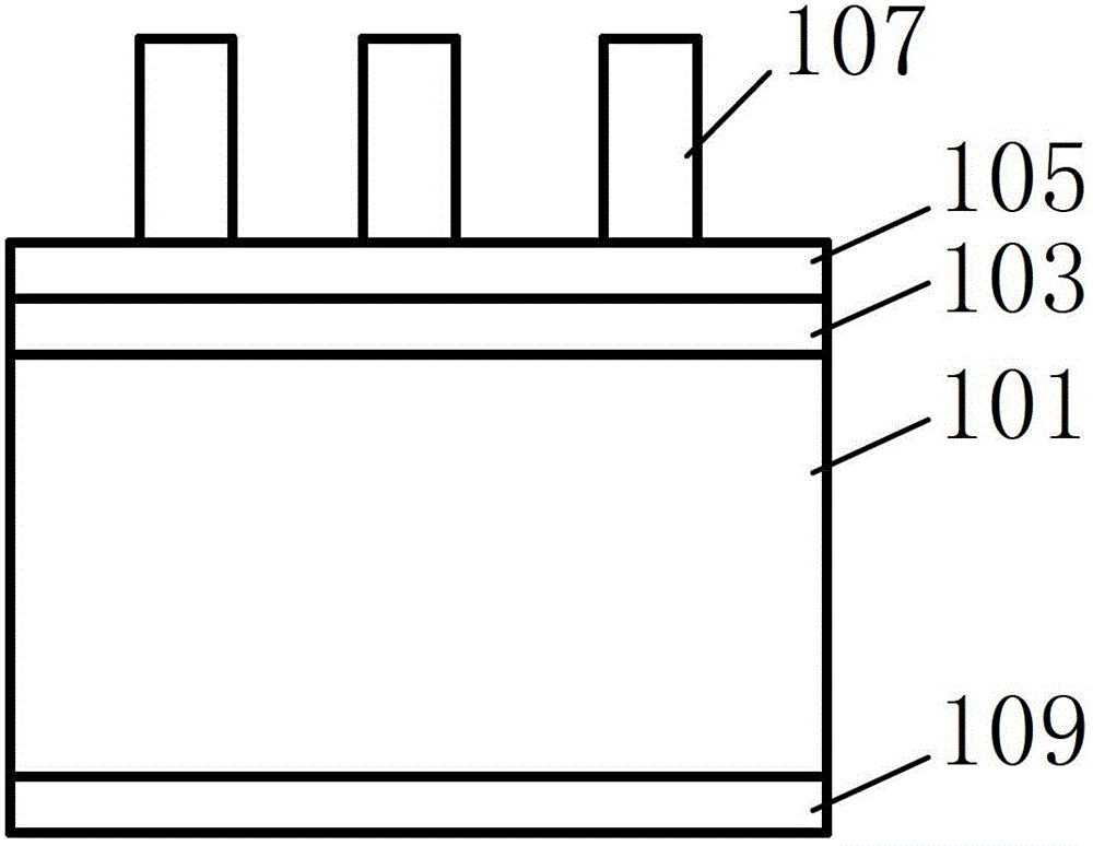
[0049] This embodiment provides a copper interconnection structure on the top layer. Generally, in the copper interconnection structure on the top layer, the thickness of the copper interconnection line can reach 16000 angstroms, while in the copper interconnection structure between layers, the thickness of the copper interconnection line is The thickness is only about 3000 angstroms, so the copper interconnection structure on the top layer is more likely to prevent the crack problem mentioned in the background art. It should be noted that the technical solution of the present invention is not only applicable to the copper interconnection structure of the top layer, but also applicable to the interlayer copper interconnection structure, so the structure disclosed in this embodiment below can be applied to the interlayer copper interconnection structure. In the interconnection structure, similarly, the structures and manufacturing methods described in the second to fourth embodi...

Embodiment 2

[0057] This embodiment continues to provide a top layer copper interconnection structure. The copper interconnection structure provided in this embodiment has many similarities with the copper interconnection structure described in Embodiment 1. For the similarities, please refer to the corresponding content in Embodiment 1. This embodiment focuses on the differences between the two to be explained.

[0058] Please refer to Image 6 , the copper interconnection structure includes a semiconductor substrate (not shown), a first interlayer dielectric layer 611 located on the semiconductor substrate, a copper plug 631 penetrating through the first interlayer dielectric layer, located on the The second interlayer dielectric layer 612 on the first interlayer dielectric layer 611 runs through the copper interconnection line 632 of the second interlayer dielectric layer 612 . In this embodiment, a barrier layer 613 is further included between the first interlayer dielectric layer 61...

Embodiment 3

[0065] This embodiment provides a method for fabricating a top-layer copper interconnection structure, including steps S31 to S38. It should be noted that in this embodiment, the steps are named from S31 to S38 to distinguish and facilitate description of the steps, but the sequence of the steps is not limited, and the sequence of the steps can be adjusted in different embodiments. Each step will be explained below, please refer to Figure 5 as well as Figure 7 to Figure 13 .

[0066] Step S31, providing a semiconductor substrate.

[0067] The semiconductor substrate provided in this embodiment refers to a semiconductor substrate that can include various types of semiconductor device structures. Although it is not shown in the figure, those skilled in the art can think that the semiconductor substrate can include the semiconductor substrate that can be fabricated in the field. Any structure on the semiconductor substrate, such as CMOS and other device structures.

[0068]...


PUM

PropertyMeasurementUnit
thicknessaaaaaaaaaa
flexural strengthaaaaaaaaaa

Abstract

The invention provides a copper interconnection structure and a method for manufacturing the same. The copper interconnection structure comprises a semiconductor substrate, a first interlayer dielectric layer disposed on the semiconductor substrate, a copper plug running through the first interlayer dielectric layer, a second interlayer dielectric layer disposed on the first interlayer dielectric layer, and a copper interconnection wire running through the second interlayer dielectric layer. A first protective layer is arranged between the first interlayer dielectric layer and the copper interconnection wire, and a second protective layer is arranged between the second interlayer dielectric layer and the copper interconnection wire. According to the copper interconnection structure provided by the invention, as the first protective layer is arranged between the first interlayer dielectric layer and the copper interconnection wire and the second protective layer is arranged between the second interlayer dielectric layer and the copper interconnection wire, direct contact between the copper interconnection wire and the first interlayer dielectric layer and between the copper interconnection wire and the second interlayer dielectric layer is avoided, and the first interlayer dielectric layer and the second interlayer dielectric layer are prevented from being fractured by the copper interconnection wire.

Description

technical field [0001] The invention relates to the field of semiconductors, in particular to a copper interconnection structure and a manufacturing method of the copper interconnection structure. Background technique [0002] With the development of semiconductor technology, the integration level of VLSI chips has reached hundreds of millions or even billions of devices, and multi-layer metal interconnection technology with more than two layers is widely used. The metal interconnection layer includes a metal interconnection structure (the metal interconnection structure includes metal interconnection lines and metal plugs) and an inter-layer dielectric layer (Inter-layer dielectric, ILD). The fabrication method of the metal interconnection layer generally includes manufacturing trenches and vias in the interlayer dielectric layer, and then depositing metal in the trenches and vias, and the deposited metal forms the metal interconnection structure. Because copper has good c...

Claims


Application Information

Patent Timeline
Patent Type & Authority Applications(China)
IPC IPC(8): H01L23/532H01L21/768
Inventor 周鸣
Owner SEMICON MFG INT (SHANGHAI) CORP
Why Eureka
Try Eureka