Method for obtaining monocrystalline silicon holocrystalline face etching rate under action of surface active agents

A surfactant and etching rate technology, applied in special data processing applications, instruments, electrical digital data processing, etc., can solve problems such as large errors, high technical requirements, and inability to explain the real reasons for silicon etching

Active Publication Date: 2015-03-25
SOUTHEAST UNIV
View PDF3 Cites 8 Cited by
  • Summary
  • Abstract
  • Description
  • Claims
  • Application Information

AI Technical Summary

Problems solved by technology

The silicon hemisphere test method can obtain the real etching rate of all crystal planes. It is a commonly used process method at present, but its test materials are expensive, the cycle is long, and the technical requirements are high. It needs precise measurement and test equipment to complete; the interpolation calculation method uses coordinate substitution The method uses a small number of crystal surface etch

Method used


Image

  • Method for obtaining monocrystalline silicon holocrystalline face etching rate under action of surface active agents
  • Method for obtaining monocrystalline silicon holocrystalline face etching rate under action of surface active agents
  • Method for obtaining monocrystalline silicon holocrystalline face etching rate under action of surface active agents

Examples


Embodiment 1

[0067] Example 1 is used to illustrate the detailed implementation steps of the present invention and the results obtained; Example 2 is used to illustrate that the present invention has wide applicability to etching systems under the action of different surfactants; Example 3 is used to illustrate surface activity Implementation effect of three-dimensional microstructure simulation of single crystal silicon under the action of agent.

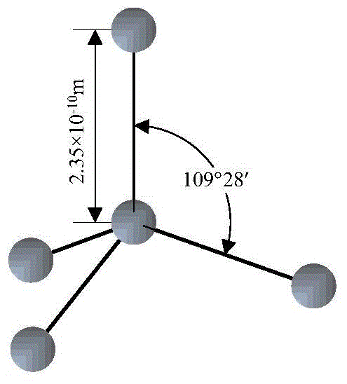
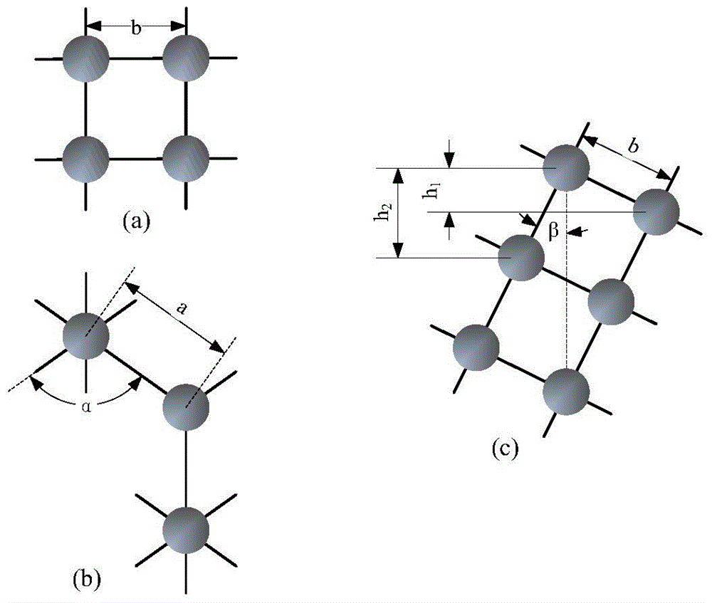
[0068] The design variables in all examples are: Nine parameters of the Monte Carlo S-AEP etch probability function: ε 11 ,ε 12 ,ε 21 ,ε 22 ,E 1 ,E 2 ,g,E m ,r 0 .

[0069] Example 1 (determination of the etching rate of any {h, k, l} crystal plane under the etching conditions of 80°C KOH+IPA):

[0070] Etching environment: 80°C, KOH (medium concentration) + IPA.

[0071] Etching object: single crystal silicon

[0072] Experimental data: 80 ℃, KOH (medium concentration) and KOH (medium concentration) + IPA etching conditions seven con...

Embodiment 2

[0185] Example 2 (25wt%TMAH+0.1%(vv)Triton, the etching rate of any {h k l} crystal plane is determined under the process condition of 80°C):

[0186] Etching environment: 25wt%TMAH+0.1%(vv)Triton, 80°C

[0187] Etching object: single crystal silicon

[0188] Experimental data: Under the etching conditions of 25wt% TMAH at 80°C and 25wt% TMAH+0.1% (vv) Triton at 80°C, the experimental etching rates of seven constrained crystal planes.

[0189] Experimental goal: Under the action of surfactant, single crystal silicon wet etching a small amount of crystal facets to obtain the etching rate of the whole crystal facets

[0190] Seven constrained crystal planes: (100), (110), (111), (331), (211), (411), (310)

[0191] The experimental etching rate (um / min) of the seven constrained crystal planes at 80°C and 25wt% TMAH:

[0192] V(100)=0.437

[0193] V(110)=0.698

[0194] V(111)=0.031

[0195] V(331)=0.919

[0196] V(211)=0.784

[0197] V(411)=0.870

[0198] V(310)=0.922

...

Embodiment 3

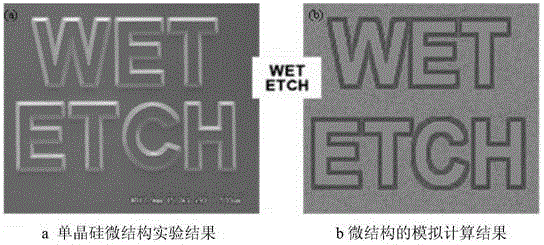
[0208] Example 3 (Calculation and simulation of three-dimensional microstructure processing of single crystal silicon under the action of surfactant)

[0209] Etching environment: 25%TMAH+0.1%(vv)Triton, 80℃;

[0210] Etching object: single crystal silicon


PUM


Abstract

The invention discloses a method for obtaining the monocrystalline silicon holocrystalline face etching rate under the action of surface active agents. The method comprises the steps that 1, the experiment etching rate of each constraint crystal face is obtained; 2, the value range of target parameters and an optimization population for generating the target parameters are determined; 3, a Monte Carlo S-AEP silicon atom removal probability function under the action of the surface active agents is built, and the etching probability of target atoms is calculated; 4, the stimulation etching rate of the constraint crystal face of each individual in the population is calculated; 5, a certain constraint crystal face is selected as a base crystal face, and the emulation etching rate of the constraint crystal face of each individual in the population is calculated; 6, the optimal individual in the population is screened out through an individual fitness evaluation method; 7, whether the emulation etching rate of the constraint crystal face of the optimal individual meets the output condition or not is judged, if yes, the optimal individual is output and a monocrystalline silicon full etching rate curve is generated, and if not, the optimal individual is encoded and subjected to heritable variation, a next generation of population is generated, and a new round of cycle is started.

Description

technical field [0001] The invention belongs to the field of microelectromechanical system (MEMS) bulk silicon conformal anisotropic wet etching processing and error control, and relates to the problem of Monte Carlo wet etching process model, specifically a small amount of single crystal under the action of surfactant The experimental etching rate of the silicon crystal plane obtains the etching rate of all arbitrary {h k l} crystal planes. Background technique [0002] Silicon wet etching is an important process for processing three-dimensional complex microstructures. In particular, the conformal anisotropic wet etching process after adding surfactants can be processed on silicon substrates depending on the difference in etching rates of different crystal planes. Many complex structures, such as cavity structure, cantilever structure, resonator, etc.; among them, the etching rate of each crystal plane of single crystal silicon is determined by the etching characteristics ...

Claims


Application Information

Patent Timeline
IPC IPC(8): G06F17/50
Inventor 幸研张辉
Owner SOUTHEAST UNIV
Why Eureka
Try Eureka