Chip separation method for 3D stacked chip encapsulator

A technology of chip packaging and separation method, which is applied in semiconductor/solid-state device manufacturing, semiconductor/solid-state device testing/measurement, electrical components, etc. Electrical measurement analysis, the effect of avoiding inclined grinding damage, avoiding forced cracking or warping damage

Active Publication Date: 2015-03-25
FIFTH ELECTRONICS RES INST OF MINIST OF IND & INFORMATION TECH
View PDF5 Cites 17 Cited by
  • Summary
  • Abstract
  • Description
  • Claims
  • Application Information

AI Technical Summary

Problems solved by technology

The mechanical unsealing method is mainly used for the unsealing of ceramic cover plate packaging or metal shell packaging devices. The material of the packaging shell is removed by grinding or prying to expose the inner cavity of the package, but this method cannot unseat the chip in the package cavity. Partial processing and leaving the leads intact
[0006] Therefore, traditional chemical etching or mechanical unsealing methods cannot meet the needs of physical analysis of ULSI non-top chip in 3D stacked chip packaging

Method used


Image

  • Chip separation method for 3D stacked chip encapsulator
  • Chip separation method for 3D stacked chip encapsulator
  • Chip separation method for 3D stacked chip encapsulator

Examples


Embodiment 1

[0038] In this embodiment, the memory containing two chips of NAND Flash+Mobile SDRAM (the two-layer chips adopt the form of cross-stacking) is taken as an example, and the second layer of chips is obtained by separation. The separation method includes the following steps (for the technical flow chart, see figure 1 ):

[0039] (1) Determine the grinding area and its area

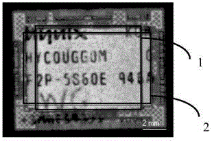
[0040] Scanning Acoustic Microscopy (C-SAM) memory internal structure such as figure 2 As shown, the memory is a cross-type double-sided lead package, in which, 1 is the first layer chip, and 2 is the second layer chip; the packaging material and 1 the first layer chip are determined to be the grinding area, and the area is 8mm; at the same time, the memory initial The thickness is about 1mm. According to experience, usually the uppermost packaging material accounts for about 1 / 3 of the total thickness of the memory, which provides a reference for the grinding force when grinding the packaging material in ...


PUM


Abstract

The invention discloses a chip separation method for a 3D stacked chip encapsulator. The method comprises the steps that acoustic scanning micro-detection is conducted on the internal structure of a 3D stacked chip encapsulated ULSI sample to determine a region to be ground and the area of the region to be ground; the 3D stacked chip encapsulated ULSI sample is fixed to a grinding table through hot molten wax; grinding is conducted, wherein a grinding drill bit, the grinding intensity and the grinding direction are selected according to the area of the ground region, an encapsulating material and chips are removed, and the region is ground to a protective layer covering the surface of a target chip; a chemical etching method is adopted to remove the protective layer. According to the chip separation method, grinding is used as a main mode, and chemical etching is used as an auxiliary mode; a specific local region is removed through grinding, and the internal structure of the lower chips and bonding wires of the lower chips are not damaged; the protective layer covering the surface of the target chip or chip binder is removed through the chemical etching method, and then the target chip is exposed; the internal structure of the obtained target chip and the bonding wire on the target chip are complete and not damaged, and therefore subsequent electrical logging analysis is facilitated.

Description

technical field [0001] The invention relates to a chip separation method, in particular to a chip separation method for a 3D stacked chip packaging device. Background technique [0002] 3D stacked chip packaging technology uses a three-dimensional space to realize multi-chip interconnection. Under the premise of not changing the size of the package, it can be stacked in the same package in the vertical direction by wire bonding or TSV interconnection. Two or more chips. 3D stacked chip packaging ultra-large-scale integration (ULSI) has greatly reduced the power consumption of the circuit while improving the circuit performance, and has become a new favorite of high-performance devices. [0003] At present, for brand new 3D ULSI products, its internal structure is sometimes checked through destructive physical analysis, which requires exposing the multi-layer chips inside the 3D ULSI layer by layer, and internal visual inspection of the internal structure of each layer, so t...

Claims


Application Information

Patent Timeline
Patent Type & Authority Applications(China)
IPC IPC(8): H01L21/02
CPCH01L21/02H01L21/304H01L21/30604H01L22/26
Inventor 林晓玲章晓文陆裕东苏菊花
Owner FIFTH ELECTRONICS RES INST OF MINIST OF IND & INFORMATION TECH
Why Eureka
Try Eureka