
Manufacturing method and structure of bipolar transistor

A kind of bipolar triode, technology of manufacturing method

Active Publication Date: 2017-03-29
SHANGHAI HUAHONG GRACE SEMICON MFG CORP
View PDF4 Cites 0 Cited by
  • Summary
  • Abstract
  • Description
  • Claims
  • Application Information

AI Technical Summary

Problems solved by technology

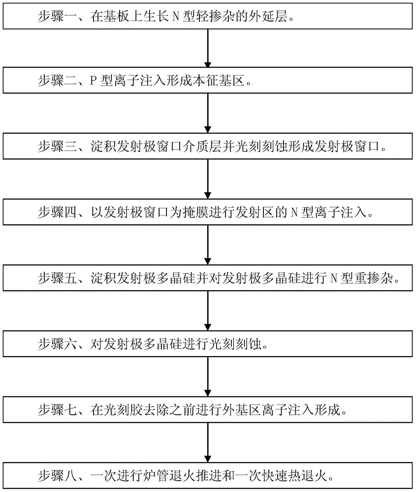
[0014] In the existing method, since both the outer base region and the emitter polysilicon are heavily doped, after the annealing of the furnace tube in step 8, the outer base region and the emitter polysilicon are heavily doped impurities that will advance to the emitter region and the base. In the PN junction region formed by the region, both the emitter region and the base region are heavily doped and formed as an abrupt junction, which reduces the breakdown voltage of the emitter-base junction and easily causes a gap between the emitter and the base. Increased tunneling leakage reduces the emitter-to-collector breakdown voltage across the device

Method used


Image

  • Manufacturing method and structure of bipolar transistor
  • Manufacturing method and structure of bipolar transistor
  • Manufacturing method and structure of bipolar transistor

Examples


Embodiment Construction

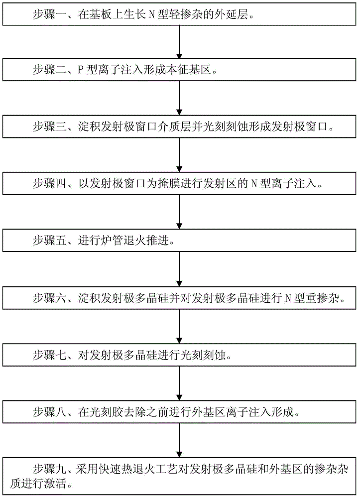
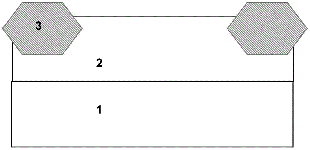
[0041] Such as figure 2 Shown is the flow chart of the method of the embodiment of the present invention; Figure 3A to Figure 3E As shown, it is a device structure diagram in each step of the method of the embodiment of the present invention; the manufacturing method of the bipolar transistor of the embodiment of the present invention includes the following steps:

[0042] Step 1, such as Figure 3A As shown, an N-type lightly doped epitaxial layer 2 is grown on an N-type heavily doped substrate 1, and the epitaxial layer 2 forms a collector region of a bipolar transistor. Preferably, the substrate 1 is a silicon substrate. The N-type lightly doped concentration of the epitaxial layer 2 is: 4E15cm -3 ~5E15cm -3 .

[0043]Field oxygen 3 is formed, said field oxygen 3 defines a contact area between said collector region and said intrinsic base region 4 .

[0044] Step two, such as Figure 3B As shown, the first P-type ion implantation is performed to form the intrinsic ...


PUM


Abstract

The invention discloses a manufacturing method of a bipolar triode. The manufacturing method includes the steps that an N-type lightly-doped epitaxial layer grows on a substrate; P-type ions are injected, and an intrinsic base region is formed; an emitter window dielectric layer is deposited and photoetched, and an emitter window is formed; the emitter window serves as a mask for injecting N-type ions in an emitter region; a furnace tube is annealed and pushed; emitter polycrystalline silicon is deposited and N-type heavy doping is conducted on the emitter polycrystalline silicon; the emitter polycrystalline silicon is photoetched; ion injection forming of an outer base region is conducted before photoresist is removed; the emitter polycrystalline silicon and doped impurities of the outer base region are activated through the rapid thermal annealing process. The invention further discloses the bipolar triode. The breakdown voltage of an emitter and a base can be increased, tunneling electric leakage between the emitter and the base is reduced, the breakdown voltage from the emitter to a collector of the whole device is increased, the process cost is low, and the cut-off frequency and the power gain of the device can be kept at high values.

Description

technical field [0001] The invention relates to the field of manufacturing semiconductor integrated circuits, in particular to a method for manufacturing a bipolar triode; the invention also relates to a bipolar triode. Background technique [0002] Bipolar transistors for conventional radio frequency applications require a cut-off frequency as high as possible under a certain breakdown voltage (BVCEO) of the collector and emitter regions. The main factors affecting the cut-off frequency are the base region and the base-collector region junction. The transit time of the formed depletion region. The cutoff frequency is inversely proportional to the transit time, which is proportional to the width of the base and junction depletion regions. The junction depletion region width is in turn proportional to the emitter-to-collector breakdown voltage. Therefore, in order to obtain a higher cut-off frequency under the same breakdown voltage, the narrower the base width is, the bett...

Claims


Application Information

Patent Timeline
Patent Type & Authority Patents(China)
IPC IPC(8): H01L21/331H01L21/265H01L29/73
CPCH01L29/66234H01L29/73
Inventor 陈曦史稼峰周正良
Owner SHANGHAI HUAHONG GRACE SEMICON MFG CORP
Learn More