

Shallow trench isolation structure and manufacturing method thereof
A technology of shallow trench isolation and manufacturing method, which is applied in the field of shallow trench isolation structure and its manufacturing, and can solve the problems of peripheral circuit etching process influence, upper edge unevenness, etc.
- Summary
- Abstract
- Description
- Claims
- Application Information
AI Technical Summary
Problems solved by technology
Method used
Image

Examples
Embodiment Construction
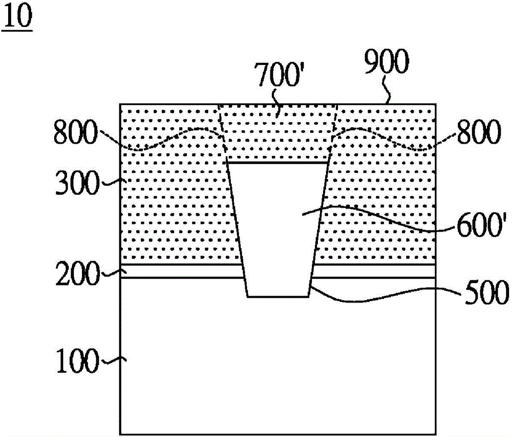
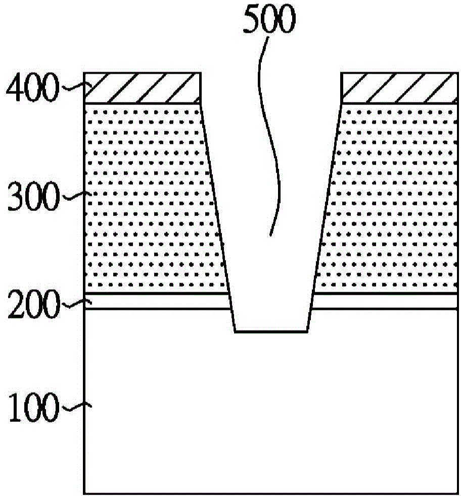
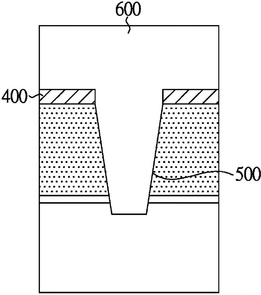
[0023] Please refer to figure 1 , which shows a shallow trench isolation structure (Shallow trench isolation structure) according to an embodiment of the present invention. The shallow trench isolation structure 10 can be applied to an array area or a peripheral area of a semiconductor device, including a substrate 100, a gate oxide layer 200, a first polysilicon layer 300, a shallow trench 500, The oxide layer 600' and the second polysilicon layer 700' are filled. The substrate 100 , the gate oxide layer 200 and the first polysilicon layer 300 are arranged in sequence, and are the base material of a semiconductor device, wherein the gate oxide layer 200 can be used as a gate of a CMOS device. The shallow trench 500 penetrates through the first polysilicon layer 300 and the gate oxide layer 200 , and stops at the substrate 100 . The filling oxide layer 600' is formed in the shallow trench 500 for isolating adjacent semiconductor devices, and the filling oxide layer 600' do...
PUM
 Abstract
Description
Claims
Application Information