Thin film transistor, preparing method of thin film transistor, array substrate, preparing method of array substrate and display device

A technology of thin-film transistors and array substrates, applied in the display field, can solve problems such as unstable performance, affecting the service life of TFTs, and short-channel effects of TFTs

Inactive Publication Date: 2015-03-25
BOE TECH GRP CO LTD
View PDF3 Cites 25 Cited by
  • Summary
  • Abstract
  • Description
  • Claims
  • Application Information

AI Technical Summary

Problems solved by technology

However, the traditional TFT only includes one gate; the gate control ability of the single-gate TFT is relatively weak, which will make the TFT prone to short-channel effects, resulting in unstable performance and further affecting the service life of the TFT

Method used


Image

  • Thin film transistor, preparing method of thin film transistor, array substrate, preparing method of array substrate and display device
  • Thin film transistor, preparing method of thin film transistor, array substrate, preparing method of array substrate and display device
  • Thin film transistor, preparing method of thin film transistor, array substrate, preparing method of array substrate and display device

Examples


preparation example Construction

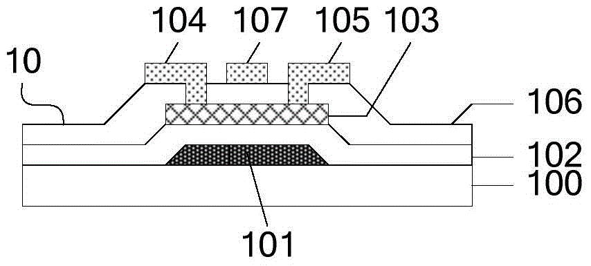
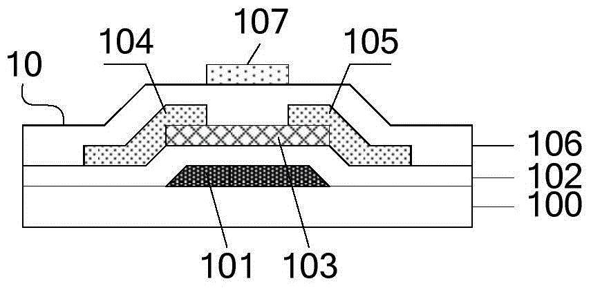
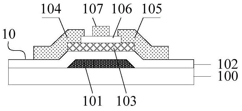
[0071] Correspondingly, an embodiment of the present invention also provides a method for manufacturing a thin film transistor 10, the method comprising: forming a first gate 101, a gate insulating layer 102 located above the first gate 101, a gate insulating layer 102 located on the gate The semiconductor active layer 103 above the insulating layer 102, the source electrode 104 and the drain electrode 105 in contact with the semiconductor active layer 103; on this basis, the method further includes: forming an interlayer insulating layer 106 and forming a second Two gates 107 ; wherein, the interlayer insulating layer 106 is formed between the second gate 107 and the semiconductor active layer 103 .

[0072] Specifically, the interlayer insulating layer 103 may be formed between the semiconductor active layer 103 and the source 104 and the drain 105 and / or formed between the source 104 and the drain 105 The side away from the semiconductor active layer 103 .

[0073] The thi...


PUM


Abstract

The embodiment of the invention provides a thin film transistor, a preparing method of the thin film transistor, an array substrate, a preparing method of the array substrate and a display device, and relates to the technical field of displaying. The grid control capability of the thin film transistor can be enhanced, the performance of the thin film transistor can be kept stable for a long time, and the service life of the thin film transistor can be further prolonged. The thin film transistor comprises a first grid electrode, a grid insulating layer located on the first grid electrode, a semiconductor active layer located on the grid insulating layer, a source electrode and a drain electrode, wherein the source electrode and the drain electrode are in contact with the semiconductor active layer. The thin film transistor further comprises an interlayer insulating layer and a second grid layer, wherein the interlayer insulating layer is arranged between the second grid electrode and the semiconductor active layer. The thin film transistor can be used for manufacturing a display component.

Description

technical field [0001] The invention relates to the field of display technology, in particular to a thin film transistor and its preparation method, an array substrate and its preparation method, and a display device. Background technique [0002] With the development of display technology, flat panel displays have gradually penetrated into people's lives. Currently common flat panel displays mainly include LCD (Liquid Crystal Display, Liquid Crystal Display) and OLED (Organic Light-Emitting Diode, Organic Light-Emitting Diode) displays. During the imaging process, each pixel unit is driven by a TFT (Thin Film Transistor, thin film transistor) integrated on the array substrate, and is controlled by a peripheral driving circuit to realize image display. [0003] In the above-mentioned displays, TFT is a switch to control image display, and is the key to realize LCD and OLED display, which is directly related to the further development of high-performance flat-panel displays....

Claims


Application Information

Patent Timeline
Patent Type & Authority Applications(China)
IPC IPC(8): H01L29/786H01L27/12H01L21/336
CPCH01L29/78645H01L21/28H01L27/1214H01L29/4232H01L29/66742
Inventor 刘翔
Owner BOE TECH GRP CO LTD
Why Eureka
Try Eureka