Electrochromic device for screening inverse opal photonic crystal structure with high flux

An electrochromic device and anti-opal technology, applied in instruments, optics, nonlinear optics, etc., can solve the problems of complex operation, low screening efficiency, high manpower and financial costs, etc., to improve screening efficiency, speed up research and development, and save cost effect

Inactive Publication Date: 2015-04-01
UNIV OF ELECTRONICS SCI & TECH OF CHINA
View PDF6 Cites 3 Cited by
  • Summary
  • Abstract
  • Description
  • Claims
  • Application Information

AI Technical Summary

Problems solved by technology

This traditional single-throughput screening has low efficiency, complex operation, long experimental cycle, and high human and financial costs.

Method used


Image

  • Electrochromic device for screening inverse opal photonic crystal structure with high flux
  • Electrochromic device for screening inverse opal photonic crystal structure with high flux
  • Electrochromic device for screening inverse opal photonic crystal structure with high flux

Examples


preparation example Construction

[0046] A method for preparing an electrochromic device for high-throughput screening of an inverse opal photonic crystal structure, comprising the following steps:

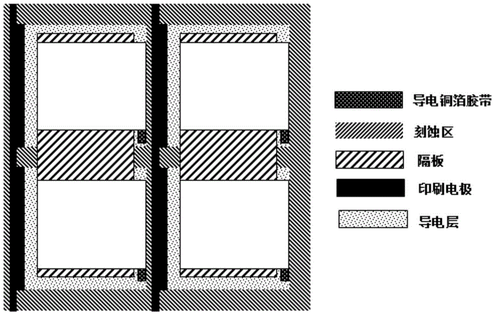
[0047] Step 1: Etch on the transparent conductive substrate to form a conductive layer arranged in an n×n matrix. Each etched strip has the same width and is insulated. After the etching is completed, clean it with sodium hydroxide, deionized water and absolute ethanol respectively. 5-10 times, then dry in an oven at 50-150°C;

[0048] Step 2: Use a screen printing machine to brush conductive paste on one row or one column of etching strips of the transparent conductive substrate obtained after the treatment in step 1, and sinter and solidify it as a printed electrode, and the printed electrode is connected to each corresponding row or column. A conductive layer is connected, the number of the printed electrodes is n, and the thickness of the printed electrodes is equal to the etching depth in step 1;
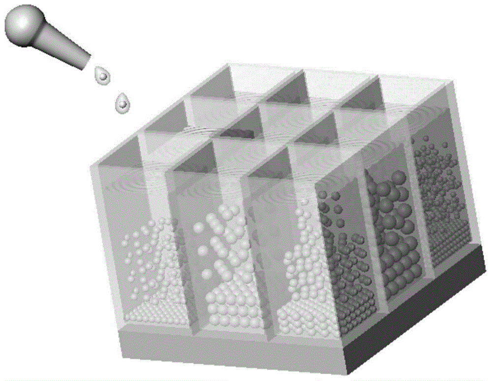
[0049] St...

Embodiment

[0058] A high-throughput screening method for electrochromic devices with an inverse opal photonic crystal structure includes the following steps:

[0059] Step 1: Use hydrochloric acid and zinc powder to etch on the ITO transparent conductive substrate to form a conductive layer arranged in a 2×2 matrix. Each etching strip has a width of 4mm and is insulated. Wash with deionized water and absolute ethanol for 5 times, and then dry in an oven at 80°C;

[0060] Step 2: Use a screen printing machine to brush conductive silver paste on a row of etching strips of the transparent conductive substrate obtained after step 1, and sinter and solidify it as a printing electrode, and the printing electrode is connected to each conductive layer corresponding to a row , the number of the printed electrodes is 2, and the thickness of the printed electrodes is equal to the etching depth in step 1;

[0061] Step 3: Place a polytetrafluoroethylene spacer on the transparent conductive substrat...


PUM

PropertyMeasurementUnit
particle diameteraaaaaaaaaa

Abstract

The invention provides an electrochromic device for screening an inverse opal photonic crystal structure with a high flux and a method of the electrochromic device, and belongs to the technical field of functional devices. The electrochromic device comprises a substrate and an electrochromic device unit which is arranged on the substrate in m*n array arrangement; the electrochromic device unit comprises working electrodes arranged on the substrate, an electrochromic film layer, an electrolyte layer and a counter electrode which are sequentially arranged from bottom to top; working electrodes in one row or one column are connected with the same printing electrode and are led out as the working electrodes; the number of the printing electrodes is m or n; the electrochromic film layer is of an inverse opal photonic crystal structure. By using the high throughput technology, a plurality of electrochromic materials and formulae can be simultaneously screened; the screening efficiency is improved; the development rate is increased; the cost is reduced.

Description

technical field [0001] The invention belongs to the technical field of functional devices, and in particular relates to an electrochromic device for high-throughput screening of an inverse opal photonic crystal structure and a preparation method thereof. Background technique [0002] With the depletion of traditional energy and the gradual deterioration of the ecological environment, it is the current and future development trend of the energy industry to develop clean energy, promote energy conservation and environmental protection, and take the road of sustainable development. Color-changing materials are new functional materials developed under this situation. Color-changing materials refer to a class of smart materials whose optical properties such as absorption, transmission, and reflection of light of different wavelengths change reversibly when external conditions (such as temperature, light, humidity, pressure, or external magnetic field, etc.) change. [0003] Elec...

Claims


Application Information

Patent Timeline
Patent Type & Authority Applications(China)
IPC IPC(8): G02F1/155G02F1/15G02F1/153
CPCG02F1/1523G02F1/134309G02F1/153G02F1/155G02F2001/15025
Inventor 吴露向勇吴刚叶涛胡琮瑾
Owner UNIV OF ELECTRONICS SCI & TECH OF CHINA
Why Eureka
Try Eureka