Flash memory structure, memory array, and programming, erasing, and reading method of flash memory structure and memory array

A technology of storage array and flash memory, which is applied in the field of storage, and can solve problems such as large space, low utilization rate of storage units, and large storage area

Inactive Publication Date: 2015-04-08
SHANGHAI HUAHONG GRACE SEMICON MFG CORP
View PDF4 Cites 10 Cited by
  • Summary
  • Abstract
  • Description
  • Claims
  • Application Information

AI Technical Summary

Problems solved by technology

[0004] The existing technology usually only uses one row of memory cells connected to the same source line to store data, which leads to low utilization of memory cells, and too many idle memory cells occupy a large space, making the memory area composed of memory cells larger , and the programming speed is slow

Method used


Image

  • Flash memory structure, memory array, and programming, erasing, and reading method of flash memory structure and memory array
  • Flash memory structure, memory array, and programming, erasing, and reading method of flash memory structure and memory array
  • Flash memory structure, memory array, and programming, erasing, and reading method of flash memory structure and memory array

Examples


Embodiment Construction

[0064] In order to make the above objects, features and advantages of the present invention more comprehensible, specific embodiments of the present invention will be described in detail below in conjunction with the accompanying drawings.

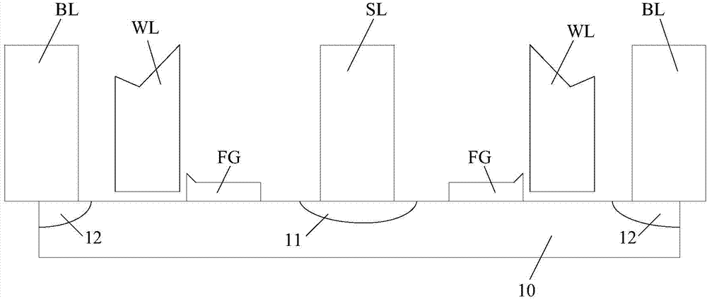
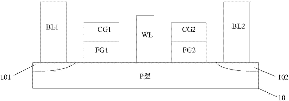
[0065] Such as figure 2 As shown, in an embodiment of the present invention, the flash memory structure may include: a semiconductor substrate 10, a bit line structure BL1, a bit line structure 2 BL2, a floating gate structure FG1, a floating gate structure FG2, a control gate structure CG1, Control gate structure 2 CG2 and word line structure WL, wherein:

[0066] The semiconductor substrate 10 has a doped well inside, including a doped well 101 and a doped well 2 102; the doped well 101 is in contact with the bit line structure 1 BL1, and the doped well 2 102 and the bit line structure 2 BL2 touch. The word line structure WL is located between the first bit line structure BL1 and the second bit line structure BL2. The first floating ...


PUM


Abstract

The invention discloses a flash memory structure, a memory array, and a programming, erasing, and reading method of the flash memory structure and the memory array. The flash memory structure comprises a semiconductor substrate, a bit line structure, a word line structure, a floating gate structure, and a control gate structure; the inner part of the semiconductor substrate is provided with a doping trap, and a source electrode and a drain electrode are formed by the doping trap; the bit line structure comprises a bit line structure 1 and a bit line structure 2 which are connected with the drain electrode and the source electrode respectively; the word line structure is arranged between the bit line structure 1 and the bit line structure 2; the floating gate structure comprises a floating gate structure 1 and a floating gate structure 2 which are arranged between the word line structure and the bit line structure respectively; the control gate structure comprises a control gate structure 1 and a control gate structure 2 which are arranged on the surface of the floating gate structure respectively; and the bit line structure, the word line structure, and the floating gate structure are all arranged on the surface of the semiconductor substrate. The flash memory structure is capable of reducing memory area, and increasing memory programming speed.

Description

technical field [0001] The invention relates to the technical field of memory, in particular to a flash memory structure, a memory array and programming, erasing and reading methods thereof. Background technique [0002] Electrically Erasable Programmable Read-Only Memory (flash memory, Electrically Erasable Programmable Read-Only Memory) is a semiconductor storage device with byte (Byte) as the minimum modification unit, which can be electronically rewritten multiple times. Compared with Erasable Programmable Read-Only Memory (EPROM, Erasable Programmable Read-Only Memory), flash memory does not need to be irradiated with ultraviolet rays or removed, and a specific voltage can be used to erase the information on the chip for writing. Enter new data. Due to the excellent performance of flash memory and the convenience of online operation, it is widely used in BIOS chips and flash memory chips that need to be frequently erased, and gradually replaces some random access memor...

Claims


Application Information

Patent Timeline
Patent Type & Authority Applications(China)
IPC IPC(8): G11C16/14G11C16/06
CPCH01L29/7881G11C16/0408G11C16/14G11C16/26G11C16/10G11C16/0425
Inventor 杨光军胡剑肖军李冰寒江红孔蔚然
Owner SHANGHAI HUAHONG GRACE SEMICON MFG CORP
Why Eureka
Try Eureka