Contact hole etching process, organic light-emitting display device and display device

A contact hole etching and contact hole technology, which is applied in semiconductor devices, electrical solid devices, semiconductor/solid device manufacturing, etc., can solve the problems of affecting the electrical performance of devices, difficult detection of etching end points, and large loss of line width. Achieve the effect of easy control of hole diameter and taper, avoid deep and difficult process holes, and reduce the difficulty of etching

Active Publication Date: 2015-04-08
KUNSHAN GO VISIONOX OPTO ELECTRONICS CO LTD
View PDF4 Cites 6 Cited by
  • Summary
  • Abstract
  • Description
  • Claims
  • Application Information

AI Technical Summary

Problems solved by technology

[0003] 1) The film layer to be etched is very thick (interlayer dielectric layer: first insulating layer ), the pore is deep and the pore diameter becomes smaller as it goes down. During the reaction process, it is easy to cause the reactant to fail to discharge in time and the etching stop phenomenon occurs; if the etching stop is avoided by prolonging the etching time or increasing the bias power (Bias Power) , it will lead to a relatively large line width loss (CD Loss), which will affect the electrical performance of the device;
[0004] 2) The end point of etching is difficult to detect, resulting in over-etching of the polysilicon layer, and a large over-etching of the polysilicon layer will affect the electrical performance of the device
Since wet etching can effectively avoid over-etching of the polysilicon layer, it needs to increase the transportation process of the device to be etched between the dry etching area and the wet etching area, and the process is cumbersome

Method used


Image

  • Contact hole etching process, organic light-emitting display device and display device
  • Contact hole etching process, organic light-emitting display device and display device
  • Contact hole etching process, organic light-emitting display device and display device

Examples


Embodiment Construction

[0030] In order to make the object, technical solution and advantages of the present invention clearer, the implementation manner of the present invention will be further described in detail below in conjunction with the accompanying drawings.

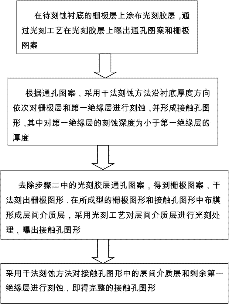
[0031] The invention provides a contact hole etching process, such as figure 1 As shown, it specifically includes the following steps:

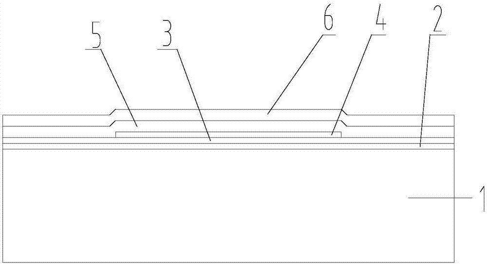
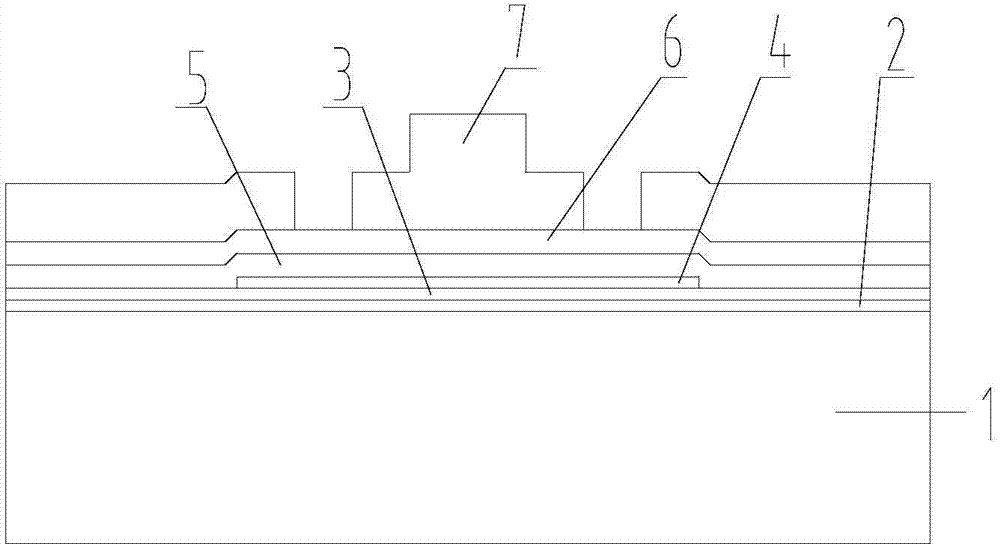
[0032] Step 1: If figure 2 As shown, a photoresist layer 7 is coated on the gate layer 6 of the substrate 1 to be etched, and a through hole pattern and a gate pattern are exposed on the photoresist layer 7 through a photolithography process.

[0033] Specifically, a Mo film layer is coated on the first insulating layer 5 by physical vapor deposition (PVD (Physical Vapor Deposition)) to form the gate layer 6, see figure 2 shown. Coating a photoresist layer 7 on the gate layer 6, and then using the Halftone (halftone image) method to expose the grid pattern and the via hole pattern on the photores...


PUM


Abstract

The invention discloses a contact hole etching hole, an organic light-emitting display device and a display device. The etching process comprises the following steps: coating a photoresist layer on a gate electrode layer to expose a through hole pattern and a gate electrode pattern; according to the through hole pattern, etching the gate electrode layer and a first insulating layer in sequence along the substrate thickness direction to form a contact hole figure, removing the through hole pattern of the photoresist layer to etch out a gate electrode figure; arranging a membrane in the molded gate electrode figure and the molded contact hole figure to form an interlayer medium layer, performing photoetching treatment on the interlayer medium layer to expose the contact hole figure; etching the interlayer medium layer and the residual first insulating layer in the contact hole figure to obtain a complete contact hole figure. The etching and molding of the contact hole can be completed only by dry-process etching, the first insulating layer at the lower layer is firstly etched and then the interlayer medium layer on the upper face is etched, so that the problems that the contact hole etching process is difficult in hole depth etching and the etching end point is difficult to detect are avoided.

Description

technical field [0001] The invention relates to the field of manufacturing flat panel display devices, in particular to a contact hole etching process, an organic light-emitting display device and a display device. Background technique [0002] At present, there are the following technical problems in the etching process of contact holes in the low temperature polysilicon technology LTPS (Low Temperature Poly-silicon) process: [0003] 1) The film layer to be etched is very thick (interlayer dielectric layer: first insulating layer ), the pore is deep and the pore diameter becomes smaller as it goes down. During the reaction process, it is easy to cause the reactant to fail to discharge in time and the etching stop phenomenon occurs; if the etching stop is avoided by prolonging the etching time or increasing the bias power (Bias Power) , it will lead to a relatively large line width loss (CD Loss), which will affect the electrical performance of the device; [0004] 2) ...

Claims


Application Information

Patent Timeline
Patent Type & Authority Applications(China)
IPC IPC(8): H01L21/768H01L21/28H01L27/32
CPCH01L21/31105H01L21/32131H01L21/768H10K59/00
Inventor 吴梦琳徐岩王冰
Owner KUNSHAN GO VISIONOX OPTO ELECTRONICS CO LTD
Why Eureka
Try Eureka