Method for etching silicon carbide shallow trench

A technology of silicon carbide and shallow trenches, which is applied in the direction of electrical components, semiconductor/solid-state device manufacturing, circuits, etc., can solve the difficulty of SiO2 mask removal, the angle of silicon carbide trench sidewall etching is difficult to achieve satisfactory results, Process errors and other issues, to achieve the effect of reducing the number of masks, reducing the difficulty of etching, and improving the angle of the side wall

Inactive Publication Date: 2019-09-24
GLOBAL ENERGY INTERCONNECTION RES INST CO LTD +1
View PDF5 Cites 2 Cited by
  • Summary
  • Abstract
  • Description
  • Claims
  • Application Information

AI Technical Summary

Problems solved by technology

[0004] It can be seen that the traditional silicon carbide trench etching method involves two etching steps. Since the two mask materials are different and the removal methods are also different, it is easy to cause process errors, introduce new impurities, etc. during the complicated preparation process. Faced with problems such as difficulty in removing the SiO2 mask, and the angle of etching the sidewall of the silicon carbide trench in the prior art is difficult to achieve satisfactory results

Method used


Image

  • Method for etching silicon carbide shallow trench
  • Method for etching silicon carbide shallow trench
  • Method for etching silicon carbide shallow trench

Examples


Embodiment Construction

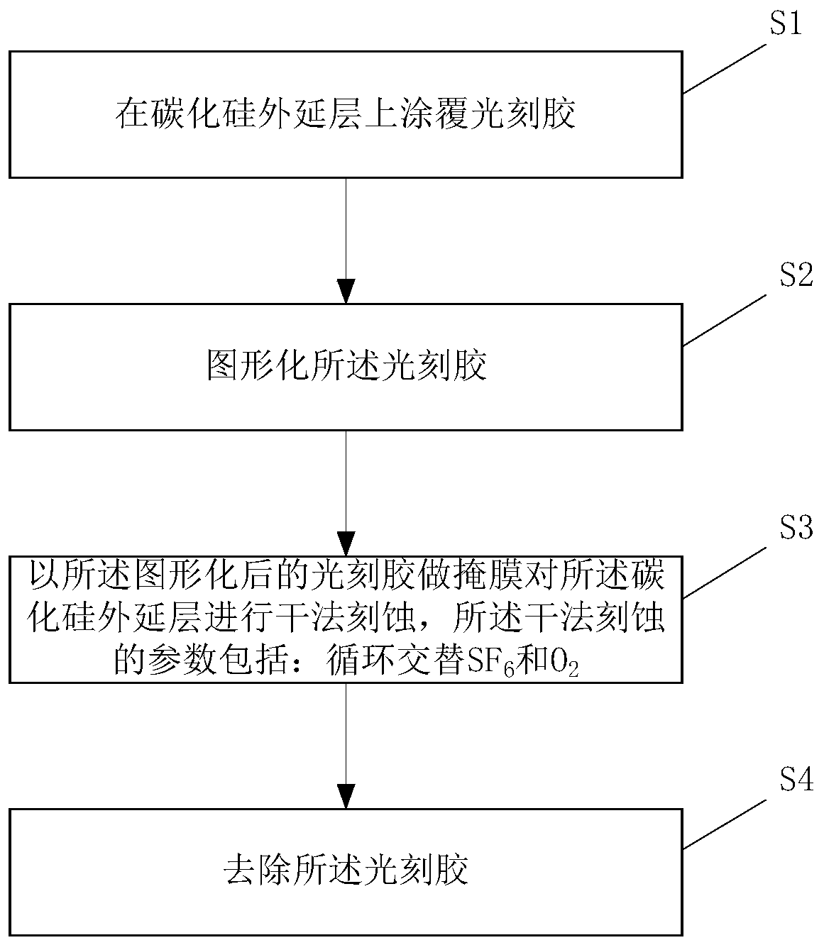
[0031] The technical solutions of the present invention will be clearly and completely described below in conjunction with the accompanying drawings. Obviously, the described embodiments are part of the embodiments of the present invention, rather than all of them. Based on the embodiments of the present invention, all other embodiments obtained by those of ordinary skill in the art without creative work shall fall within the protection scope of the present invention.

[0032] The invention provides a method for etching a silicon carbide shallow trench, such as figure 1 As shown, the method can include the following steps:

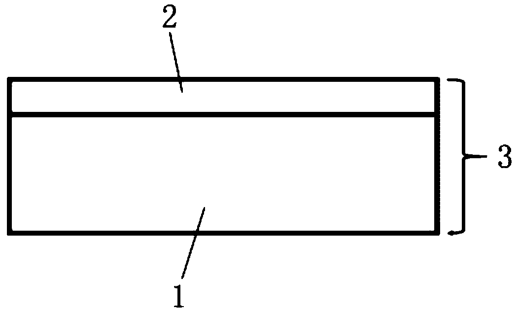
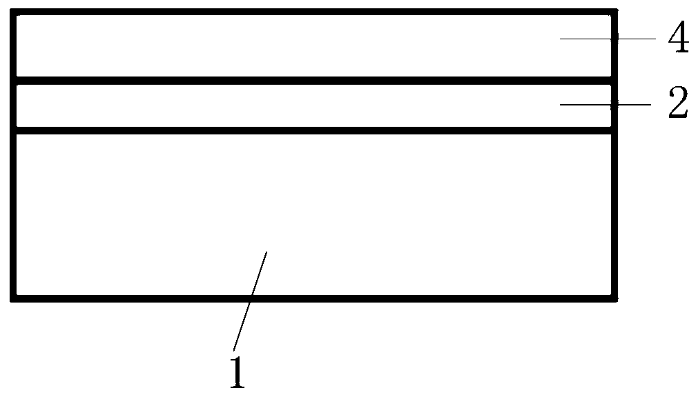
[0033] S1. Coating photoresist 4 on the silicon carbide epitaxial layer 2. Such as Figure 2 ~ Figure 3 Firstly, one or more silicon carbide epitaxial layers 2 are grown on silicon carbide substrate 1, and then RCA standard cleaning is performed on silicon carbide sample 3, and finally a layer of adhesive is coated on silicon carbide sample 3 and then coated ...


PUM


Abstract

The invention discloses a method for etching a silicon carbide shallow trench, which comprises the steps of coating a silicon carbide epitaxial layer with a photoresist; patterning the photoresist; performing dry etching on the silicon carbide epitaxial layer by taking the patterned photoresist as a mask, wherein the parameters of the dry etching include SF6 and O2 which are cyclically and alternately introduced; and removing the photoresist. According to the method provided by the embodiment of the invention for etching the silicon carbide shallow trench, the silicon carbide epitaxial layer is coated with the photoresist, and the etching is performed by directly taking the photoresist as a mask, so that the number of masks is reduced, the etching efficiency is improved, the etching difficulty is reduced, and the batch production cost of silicon carbide devices is effectively reduced. The gases SF6 and O2 are cyclically and alternately act on the material, so that the etching rate of the photoresist can be reduced on one hand, and the side wall angle of the silicon carbide trench is facilitated to be improved on the other hand.

Description

Technical field [0001] The invention relates to the field of semiconductor devices, in particular to a silicon carbide trench etching method. Background technique [0002] The electrical parameters of the third-generation semiconductor SiC material and the traditional semiconductor substrate material (Si) are very different. SiC material has large thermal conductivity, wide band gap, high electron saturation velocity and breakdown voltage, and low dielectric constant. These characteristics determine its use in high-temperature, high-frequency, and high-power semiconductor devices. The application potential of the current semiconductor field is gradually shifting to silicon carbide materials. Because the physical parameters of silicon carbide materials and silicon materials are quite different, it is impossible to apply the process preparation scheme of traditional silicon substrate materials. This patent proposes an etching process plan for silicon carbide materials. The main r...

Claims


Application Information

Patent Timeline
Patent Type & Authority Applications(China)
IPC IPC(8): H01L21/3065H01L21/027
CPCH01L21/027H01L21/3065H01L21/30655H01L21/308
Inventor 刘瑞吴昊田亮李嘉琳孙俊敏张红丹焦倩倩
Owner GLOBAL ENERGY INTERCONNECTION RES INST CO LTD
Why Eureka
Try Eureka