Contact window structure, metal plug and forming method thereof, and semiconductor structure

A technology of metal plugs and contact windows, which is applied in semiconductor devices, semiconductor/solid-state device manufacturing, semiconductor/solid-state device components, etc., can solve the problems of reduced circuit performance requirements, reduced contact area of ​​metal layers, etc., and achieves increased contact area. The effect of increasing and reducing the contact resistance

Pending Publication Date: 2022-03-29
CHANGXIN MEMORY TECH INC
View PDF0 Cites 2 Cited by
  • Summary
  • Abstract
  • Description
  • Claims
  • Application Information

AI Technical Summary

Problems solved by technology

In the process of miniaturization, the performance of the circuit requirements put forward by the design side will also be compromised
In addition, the size of the botto...

Method used


Image

  • Contact window structure, metal plug and forming method thereof, and semiconductor structure
  • Contact window structure, metal plug and forming method thereof, and semiconductor structure
  • Contact window structure, metal plug and forming method thereof, and semiconductor structure

Examples


Embodiment Construction

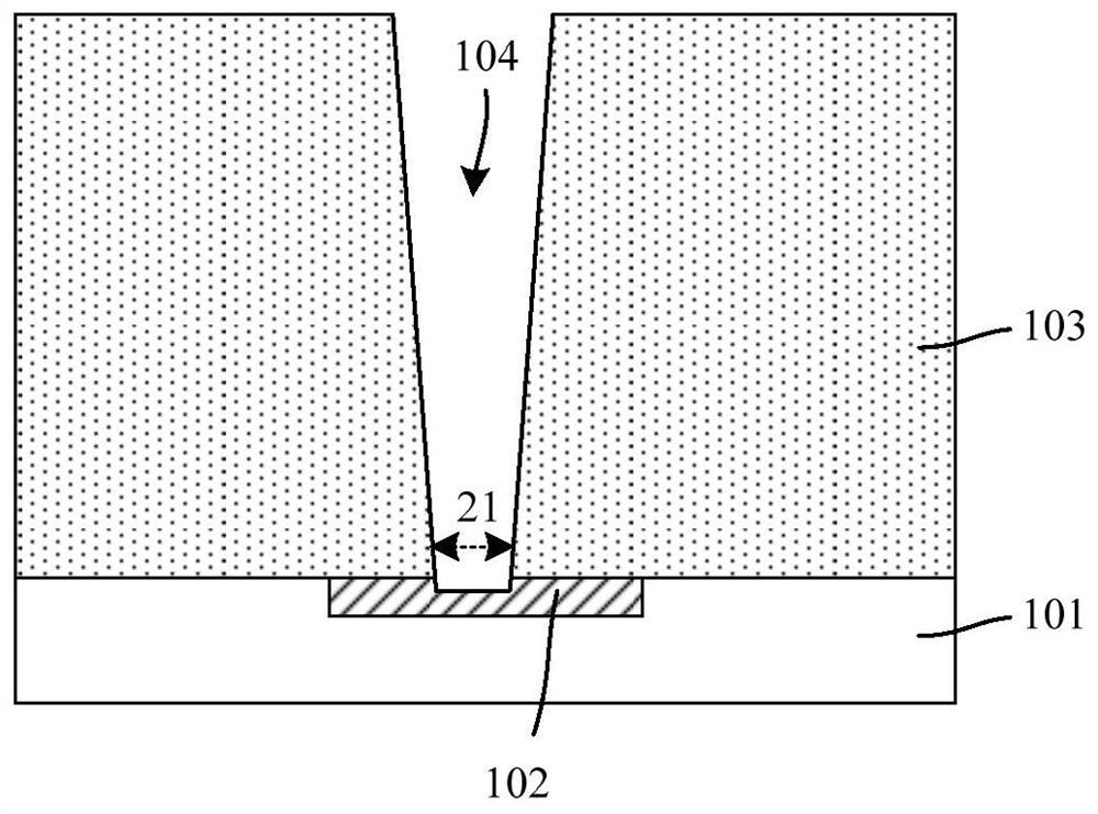
[0052] As mentioned in the background art, the shrinkage phenomenon occurs in the process of forming through holes, especially through holes with high aspect ratio. This phenomenon causes the size of the bottom of the through hole to be smaller than that of the top, and increases the contact resistance.

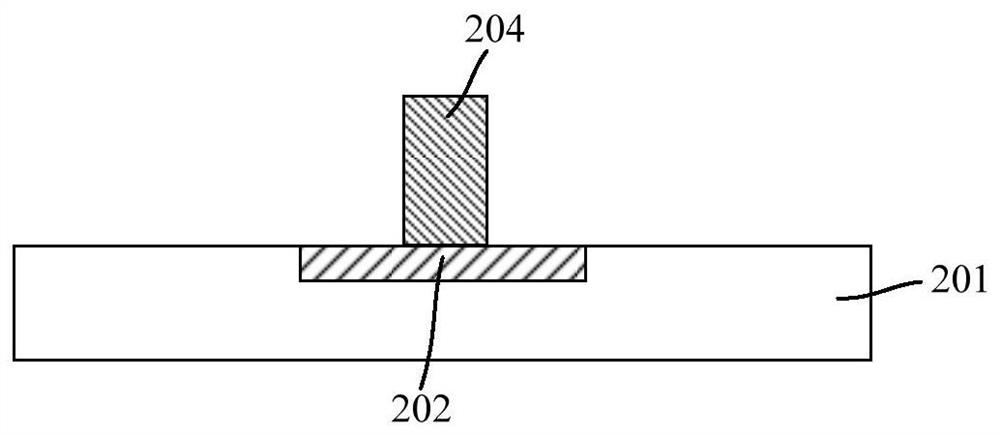
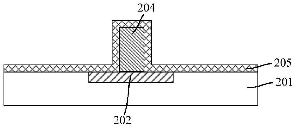
[0053]To this end, the present invention provides a contact window structure, a metal plug and a method for forming the same, and a semiconductor structure. The method for forming the contact window structure provides a target layer; an annular gasket is formed on the surface of the target layer, and the A central through hole that exposes part of the surface of the target layer is provided in the middle of the annular spacer; a dielectric layer covering the target layer and the annular spacer is formed; the dielectric layer is etched, and an etched hole communicating with the central through hole is formed in the dielectric layer. Etching holes; removing the annular spacer to...


PUM


Abstract

The invention discloses a contact window structure, a metal plug and a forming method thereof, the forming method of the contact window structure and a semiconductor structure, an annular gasket is formed on the surface of a target layer, and the middle of the annular gasket is provided with a central through hole exposing part of the surface of the target layer; forming a dielectric layer covering the substrate, the target layer and the annular gasket; etching the dielectric layer, and forming an etching hole communicated with the central through hole in the dielectric layer; and the annular gasket is removed along the etching hole and the central through hole, so that the size of the central through hole is enlarged, and the etching hole and the central through hole with the enlarged size form a contact window structure. Through the formed annular gasket, when the contact window structure is formed and the annular gasket is removed, the size of the central through hole can be increased, so that the size of the bottom of the contact window structure can be increased, and when a metal plug is formed in the contact window structure, the contact area between the bottom of the metal plug and a target layer is increased; and the contact resistance between the two is reduced.

Description

technical field [0001] The invention relates to the field of semiconductors, in particular to a contact window structure, a metal plug and a method for forming the same, and a semiconductor structure. Background technique [0002] With the development of integrated circuits to ultra-large-scale integrated circuits, the circuit density inside integrated circuits is increasing, and the number of components contained is also increasing. This development makes the surface of the wafer unable to provide enough area to manufacture the required interconnecting wires. [0003] In order to meet the requirements of interconnection lines after shrinking components, the design of two or more layers of multilayer metal interconnection lines has become a method commonly used in VLSI technology. At present, the conduction between different metal layers or metal layers and pad layers can be realized through metal plugs, refer to figure 1 , the formation of the metal plug includes: forming...

Claims


Application Information

Patent Timeline
IPC IPC(8): H01L21/768H01L23/48
CPCH01L21/76805H01L21/76895H01L21/76877H01L23/481H01L21/76816H01L2221/1063H01L23/5226
Inventor 刘杰吴秉桓应战
Owner CHANGXIN MEMORY TECH INC
Why Eureka
Try Eureka