Semiconductor structure and preparation method thereof

A semiconductor and stacked structure technology, applied in semiconductor devices, electrical solid devices, electrical components, etc., can solve the problems of gate layer breakdown, complex etching process of contact holes, high cost, etc., to save costs, reduce etching difficulty, The effect of improving performance

Active Publication Date: 2020-10-13
YANGTZE MEMORY TECH CO LTD
View PDF10 Cites 2 Cited by
  • Summary
  • Abstract
  • Description
  • Claims
  • Application Information

AI Technical Summary

Problems solved by technology

[0005] In view of the above-mentioned shortcomings of the prior art, the purpose of the present invention is to provide a semiconductor structure and its preparation method, which are used to solve the problem of complicated contact hole etching process, high cost and easy to cause gate Technical Problems of Electrode Breakdown

Method used


Image

  • Semiconductor structure and preparation method thereof
  • Semiconductor structure and preparation method thereof
  • Semiconductor structure and preparation method thereof

Examples


Embodiment 1

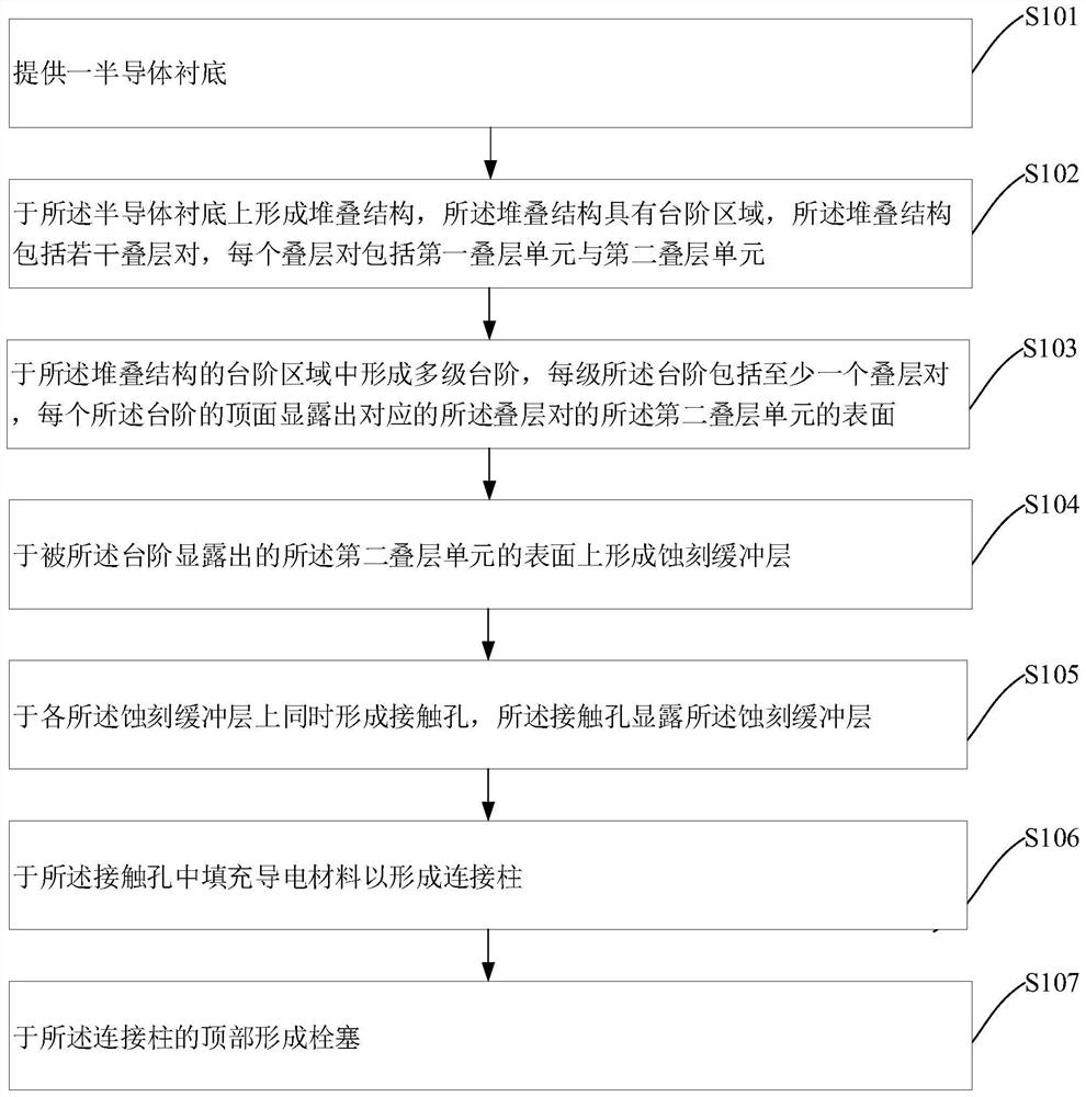
[0112] figure 1 A flow chart of the fabrication of the semiconductor structure of the embodiment of the present invention is shown. see figure 1 , the semiconductor structure method includes:

[0113] Step S101, providing a semiconductor substrate;

[0114] Step S102, forming a stacked structure on the semiconductor substrate, the stacked structure has a stepped region, the stacked structure includes several stacked pairs, each stacked pair includes a first stacked unit and a second stacked unit;

[0115] Step S103, forming multiple steps in the step area of ​​the stacked structure, each level of the steps includes at least one stacked pair, and the top surface of each level of the steps reveals the corresponding first layer of the stacked pair. The surface of the second stack unit;

[0116] Step S104, forming an etching buffer layer on the surface of the second stack unit exposed by the step;

[0117] Step S105, simultaneously forming contact holes on each of the etching...

Embodiment 2

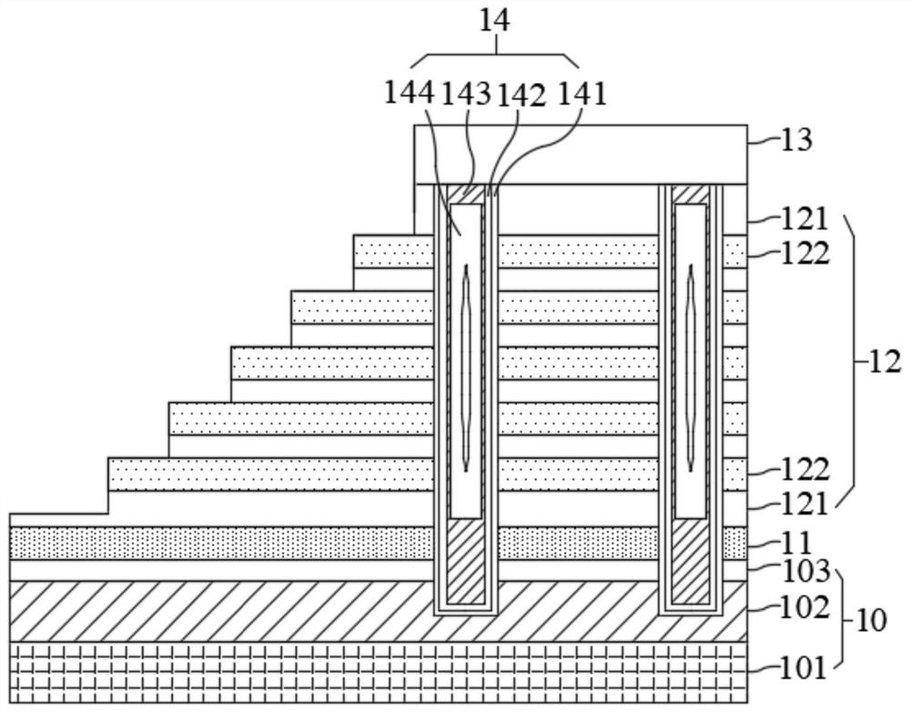
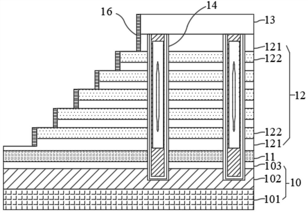
[0152] see Figure 15 , the present invention also provides a semiconductor structure prepared by the preparation method in Embodiment 1, the semiconductor structure at least includes a semiconductor substrate 10, an epitaxial layer 28, a gate stack structure 30, multi-level steps, and an etching buffer layer 18 And some connecting columns 21 ( figure 2 CT in ).

[0153] see Figure 15 , in this embodiment, the semiconductor substrate 10 includes a substrate body 101, and a doped well 102 is formed in the substrate body 101 by a doping process. The substrate body 101 can be selected according to the actual requirements of the device, and the substrate body 101 can include silicon lining, germanium (Ge) substrate, silicon germanium (SiGe) substrate, SOI (Silicon-on-insulator, silicon-on-insulator) substrate or GOI (Germanium-on-Insulator, germanium-on-insulator) substrate, etc., the substrate body 101 can also be a substrate including other element semiconductors or compoun...


PUM


Abstract

The invention provides a semiconductor structure and a preparation method thereof. The preparation method comprises the following steps: providing a semiconductor substrate; forming a stack structureon the semiconductor substrate, the stack structure comprising a plurality of stack pairs, each stack pair comprising a first stack unit and a second stack unit; forming a step structure in the stacked structure, the step structure comprising multiple steps, each step comprising at least one stacked layer pair, and the top surface of each step exposing the surface of the second stacked layer unitof the corresponding stacked layer pair; forming an etching buffer layer on the surface of the second lamination unit exposed by the step; and forming contact holes in the etching buffer layers at thesame time, wherein the contact holes expose the etching buffer layers. According to the invention, by arranging the etching buffer layer on the surface of the step, etching of all the contact holes can be completed simultaneously in one etching process, so that the process steps are simplified, the etching difficulty of the contact holes is reduced, and the cost is saved.

Description

technical field [0001] The invention belongs to the field of semiconductor design and manufacture, and in particular relates to a semiconductor structure and a preparation method thereof. Background technique [0002] In general, a three-dimensional memory includes a gate stack structure formed by alternately stacking gate layers and interlayer dielectric layers, and a contact column (Contact, CT for short) is electrically connected to the gate in a step region of the gate stack structure. However, in the actual manufacturing process of the three-dimensional memory, in order to achieve a good electrical connection between the connecting column and the gate layer in the stacked structure, it is first necessary to etch a contact hole in the dielectric layer covering the stacked gate structure until the contact hole is formed. The hole exposes the surface of the gate layer in the step region, and then the contact hole is filled with a metal material for forming a connecting col...

Claims


Application Information

Patent Timeline
Patent Type & Authority Applications(China)
IPC IPC(8): H01L27/1157H01L27/11582
CPCH10B43/35H10B43/27
Inventor 张坤王迪周文犀夏志良
Owner YANGTZE MEMORY TECH CO LTD
Why Eureka
Try Eureka