Image pickup element, method of manufacturing image pickup element, and electronic apparatus

A technology for image pickup components and pixels, which is applied in semiconductor/solid-state device manufacturing, electrical components, image communication, etc., can solve problems such as dark current and extinction, and achieve the effect of improving the interface state and suppressing dark current

Active Publication Date: 2015-04-15
SONY CORP
View PDF4 Cites 8 Cited by
  • Summary
  • Abstract
  • Description
  • Claims
  • Application Information

AI Technical Summary

Problems solved by technology

Due to recombination of electron-hole pairs generated in the photoelectric conversion part, crystal defects and dangling bonds cause extinction, or cause generation of dark current

Method used


Image

  • Image pickup element, method of manufacturing image pickup element, and electronic apparatus
  • Image pickup element, method of manufacturing image pickup element, and electronic apparatus
  • Image pickup element, method of manufacturing image pickup element, and electronic apparatus

Examples


Embodiment Construction

[0024] Hereinafter, embodiments of the present disclosure will be described in detail with reference to the accompanying drawings. It should be noted that description will be made in the following order.

[0025] 1. Embodiment (Example in which the fixed-charge film has a multilayer structure, and each layer is formed using a different manufacturing method)

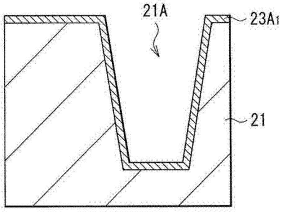
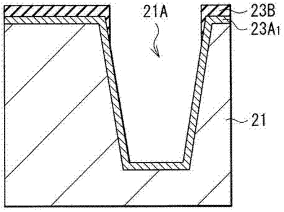
[0026] 2. Improvement (Example in which the light-shielding film is also provided in the pixel separation groove)

[0027] 3. Application examples (Application examples of solid-state image pickup devices and electronic equipment)

[0028] 1. Example

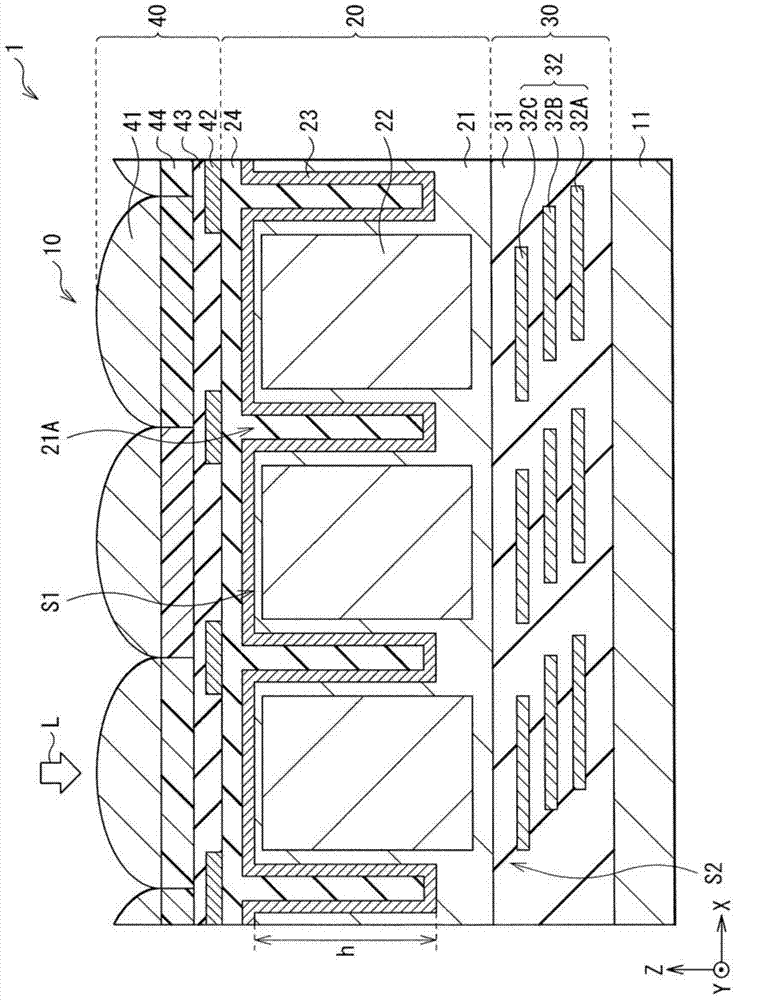
[0029] figure 1 A cross-sectional configuration of an image pickup element (image pickup element 10 ) according to an embodiment of the present disclosure is shown. The image pickup element 10 may constitute, for example, one pixel (for example, pixel P) in an image pickup device (image pickup device 1) such as a CCD image sensor and a CMOS image sensor (see Figure 5 ...


PUM


Abstract

An image pickup element includes: a semiconductor substrate including a photoelectric conversion section for each pixel; a pixel separation groove provided in the semiconductor substrate; and a fixed charge film provided on a light-receiving surface side of the semiconductor substrate, wherein the fixed charge film includes a first insulating film and a second insulating film, the first insulating film being provided contiguously from the light-receiving surface to a wall surface and a bottom surface of the pixel separation groove, and the second insulating film being provided on a part of the first insulating film, the part corresponding to at least the light-receiving surface.

Description

technical field [0001] The present disclosure relates to an image pickup element having a fixed charge film on a semiconductor substrate, a method of manufacturing such an image pickup element, and electronic equipment including such an image pickup element. Background technique [0002] In a solid-state image pickup device (image pickup device), such as a charge-coupled device (CCD) image sensor and a complementary metal-oxide-semiconductor (CMOS) image sensor, a solid-state image pickup element (image pickup device) including a photoelectric conversion portion is provided for each pixel. element). The photoelectric conversion portion of the image pickup element is composed of, for example, a semiconductor material such as silicon (Si). On the surface of the photoelectric conversion portion, there are crystal defects and dangling bonds due to destruction of the crystal structure. Crystal defects and dangling bonds cause extinction due to recombination of electron-hole pai...

Claims


Application Information

Patent Timeline
IPC IPC(8): H01L27/146
CPCH01L27/1463H01L27/14689H01L27/14621H01L27/14623H01L27/14627H01L27/1464H01L27/14636H01L27/14641H01L27/14645H01L27/14685H01L27/14603H01L27/1462H01L27/14643H04N25/75
Inventor 万田周治桧山晋志贺康幸
Owner SONY CORP
Why Eureka
Try Eureka