Liquid crystal display panel and array substrate thereof

一种阵列基板、基体的技术,应用在光学、仪器、电气元件等方向,能够解决不利液晶显示面板窄边框设计等问题,达到利于窄边框设计、减少面积的效果

Inactive Publication Date: 2015-04-22
TCL CHINA STAR OPTOELECTRONICS TECH CO LTD
View PDF3 Cites 21 Cited by
  • Summary
  • Abstract
  • Description
  • Claims
  • Application Information

AI Technical Summary

Problems solved by technology

Among them, in order to make the gate lines of this bank output high-level signals, it is necessary to ensure a large enough capacitance, that is, the area occupied by the capacitance on the array substrate, but the capacitance with a large area is not conducive to the narrow frame design of the liquid crystal display panel

Method used


Image

  • Liquid crystal display panel and array substrate thereof
  • Liquid crystal display panel and array substrate thereof
  • Liquid crystal display panel and array substrate thereof

Examples


Embodiment Construction

[0019] The technical solutions in the embodiments of the present invention will be clearly and completely described below in conjunction with the accompanying drawings in the embodiments of the present invention. Obviously, the embodiments described below are only part of the embodiments of the present invention, not all of them. Example. Based on the embodiments of the present invention, all other embodiments obtained by persons of ordinary skill in the art without creative efforts fall within the protection scope of the present invention.

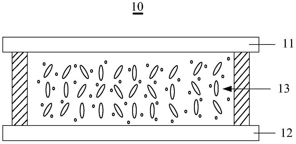
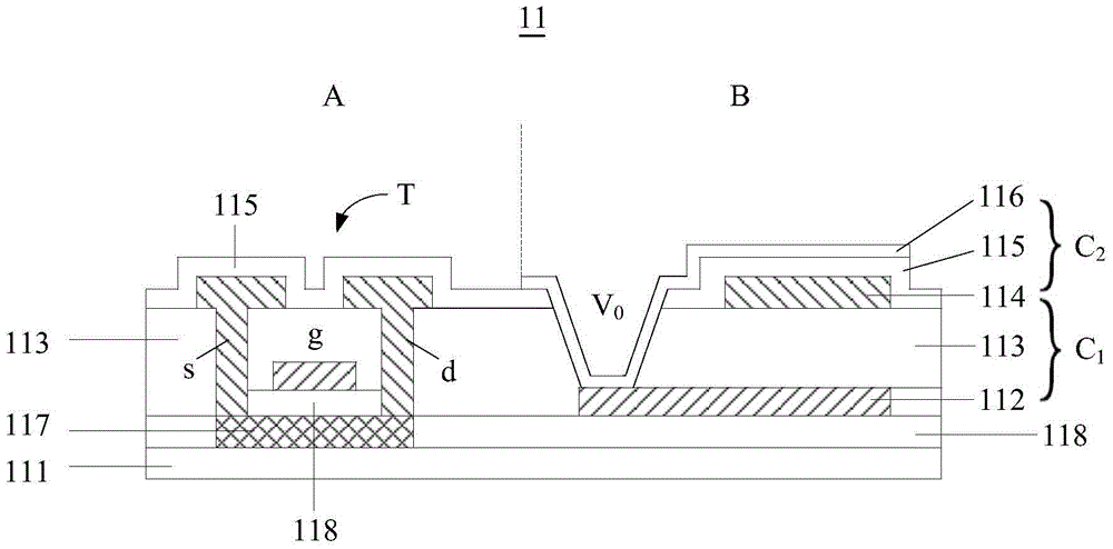
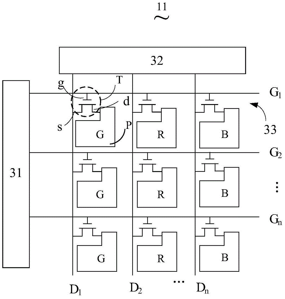
[0020] figure 1 It is a structural schematic diagram of an embodiment of the liquid crystal display panel of the present invention. Such as figure 1 As shown, the liquid crystal display panel 10 includes a first substrate 11, a second substrate 12, and a liquid crystal layer 13, and the first substrate 11 and the second substrate 12 are relatively spaced apart, wherein the second substrate 12 can be a CF (Color Filter, color filter) fi...


PUM


Abstract

The invention provides a liquid crystal display panel and an array substrate of the liquid crystal display panel. The array substrate comprises a base body, a first metal layer, a first dielectric layer, a second metal layer, an insulation layer and an electrode layer, and the first metal layer, the first dielectric layer, the second metal layer, the insulation layer and the electrode layer are formed on the base body. A first capacitor is formed by the first metal layer, the first dielectric layer and the second metal layer, a second capacitor is formed by the second metal layer, the insulation layer and the electrode layer, and the electrode layer penetrates through a channel hole of the first dielectric layer and the insulation layer to be connected with the first metal layer so that the first capacitor and the second capacitor can be connected in parallel. In this way, the occupied area of a GOA circuit on the array substrate can be reduced, and the narrow frame design of the liquid crystal display panel is facilitated.

Description

technical field [0001] The present invention relates to the technical field of liquid crystal display, in particular to a liquid crystal display panel and an array substrate thereof. Background technique [0002] Currently, more and more liquid crystal display devices adopt gate driver on array (GOA) technology to reduce the frame width of the array substrate to meet the narrow frame design trend of liquid crystal display devices. [0003] The GOA circuit in the prior art is usually composed of a plurality of shift register units, each shift register unit is connected to a gate line, and the capacitor in the shift register unit is charged by using the high-level signal output by the gate line of the previous row, So that the gate line of this row outputs a high-level signal, and then uses the high-level signal output by the gate line of the next row to realize reset. Among them, in order to make the gate lines of this bank output high-level signals, it is necessary to ensur...

Claims


Application Information

Patent Timeline
Patent Type & Authority Applications(China)
IPC IPC(8): G02F1/1362G02F1/1333
CPCG02F1/136213G02F1/136227G02F1/1368H01L27/124G02F1/13338G02F1/136286G02F1/13685H01L27/1255G02F1/1333G02F1/13454G02F1/1362G02F1/136295
Inventor 郝思坤
Owner TCL CHINA STAR OPTOELECTRONICS TECH CO LTD
Why Eureka
Try Eureka